
The NVIDIA Grace Hopper Superchip Architecture is the first true heterogeneous accelerated platform for high-performance computing (HPC) and AI workloads. It accelerates applications with the strengths of both GPUs and CPUs while providing the simplest and most productive distributed heterogeneous programming model to date. Scientists and engineers can focus on solving the world’s most important problems.
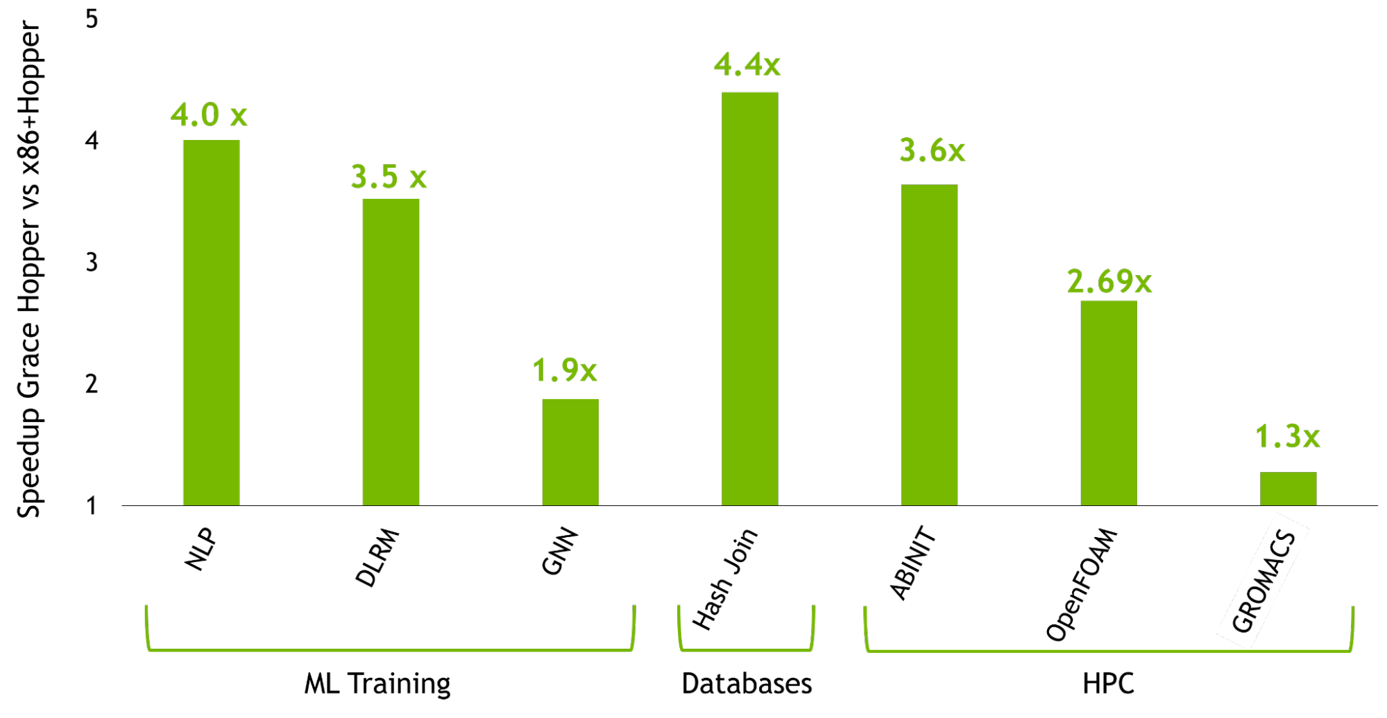
In this post, you learn all about the Grace Hopper Superchip and highlight the performance breakthroughs that NVIDIA Grace Hopper delivers. For more information about the speedups that Grace Hopper achieves over the most powerful PCIe-based accelerated platforms using NVIDIA Hopper H100 GPUs, see the NVIDIA Grace Hopper Superchip Architecture whitepaper.
Performance and productivity for strong-scaling HPC and giant AI workloads
The NVIDIA Grace Hopper Superchip architecture brings together the groundbreaking performance of the NVIDIA Hopper GPU with the versatility of the NVIDIA Grace CPU, connected with a high bandwidth and memory coherent NVIDIA NVLink Chip-2-Chip (C2C) interconnect in a single superchip, and support for the new NVIDIA NVLink Switch System.
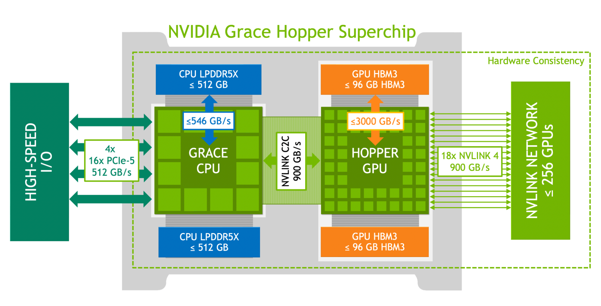
NVIDIA NVLink-C2C is an NVIDIA memory coherent, high-bandwidth, and low-latency superchip interconnect. It is the heart of the Grace Hopper Superchip and delivers up to 900 GB/s total bandwidth. This is 7x higher bandwidth than x16 PCIe Gen5 lanes commonly used in accelerated systems.
NVLink-C2C memory coherency increases developer productivity and performance and enables GPUs to access large amounts of memory.CPU and GPU threads can now concurrently and transparently access both CPU– and GPU-resident memory, enabling you to focus on algorithms instead of explicit memory management.
Memory coherency enables you to transfer only the data you need, and not migrate entire pages to and from the GPU. It also enables lightweight synchronization primitives across GPU and CPU threads by enabling native atomic operations from both the CPU and GPU. NVLink-C2C with Address Translation Services (ATS) leverages the NVIDIA Hopper Direct Memory Access (DMA) copy engines for accelerating bulk transfers of pageable memory across host and device.
NVLink-C2C enables applications to oversubscribe the GPU’s memory and directly utilize NVIDIA Grace CPU’s memory at high bandwidth. With up to 512 GB of LPDDR5X CPU memory per Grace Hopper Superchip, the GPU has direct high-bandwidth access to 4x more memory than what is available with HBM. Combined with the NVIDIA NVLink Switch System, all GPU threads running on up to 256 NVLink-connected GPUs can now access up to 150 TB of memory at high bandwidth. Fourth-generation NVLink enables accessing peer memory using direct loads, stores, and atomic operations, enabling accelerated applications to solve larger problems more easily than ever.
Together with NVIDIA networking technologies, Grace Hopper Superchips provide the recipe for the next generation of HPC supercomputers and AI factories. Customers can take on larger datasets, more complex models, and new workloads, solving them more quickly than before.
The main innovations of the NVIDIA Grace Hopper Superchip are as follows:
- NVIDIA Grace CPU:
- Up to 72x Arm Neoverse V2 cores with Armv9.0-A ISA and 4×128-bit SIMD units per core.
- Up to 117 MB of L3 Cache.
- Up to 512 GB of LPDDR5X memory delivering up to 546 GB/s of memory bandwidth.
- Up to 64x PCIe Gen5 lanes.
- NVIDIA Scalable Coherency Fabric (SCF) mesh and distributed cache with up to 3.2 TB/s memory bandwidth.
- High developer productivity with a single CPU NUMA node.
- NVIDIA Hopper GPU:
- Up to 144 SMs with fourth-generation Tensor Cores, Transformer Engine, DPX, and 3x higher FP32 and FP64 throughout compared to the NVIDIA A100 GPU.
- Up to 96 GB of HBM3 memory delivering up to 3000 GB/s.
- 60 MB L2 Cache.
- NVLink 4 and PCIe 5.
- NVIDIA NVLink-C2C:
- Hardware-coherent interconnect between the Grace CPU and Hopper GPU.
- Up to 900 GB/s total bandwidth, 450 GB/s/dir.
- The Extended GPU Memory feature enables the Hopper GPU to address all CPU memory as GPU memory. Each Hopper GPU can address up to 608 GB of memory within a superchip.
- NVIDIA NVLink Switch System:
- Connects up to 256x NVIDIA Grace Hopper Superchips using NVLink 4.
- Each NVLink-connected Hopper GPU can address all HBM3 and LPDDR5X memory of all superchips in the network, for up to 150 TB of GPU addressable memory.
Programming model for performance, portability, and productivity
Traditional heterogeneous platforms with PCIe-connected accelerators require users to follow a complex programming model that involves manually managing device memory allocations and data transfer to and from the host.
The NVIDIA Grace Hopper Superchip platform is heterogeneous and easy to program, and NVIDIA is committed to making it accessible to all developers and applications, independent of the programming language of choice.
Both the Grace Hopper Superchip and the platform are built to enable you to pick the right language for the task at hand, and the NVIDIA CUDA LLVM Compiler APIs enable you to bring your preferred programming language to the CUDA platform with the same level of code-generation quality and optimizations as NVIDIA compilers and tools.
The languages provided by NVIDIA for the CUDA platform (Figure 3) include accelerated standard languages like ISO C++, ISO Fortran, and Python. The platform also supports directive-based programming models like OpenACC, OpenMP, CUDA C++, and CUDA Fortran. The NVIDIA HPC SDK supports all these approaches, along with a rich set of accelerated libraries and tools for profiling and debugging.
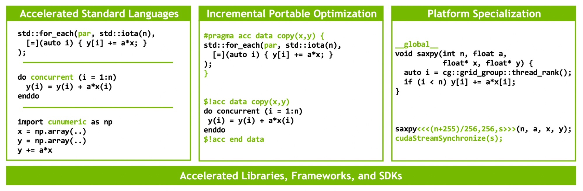
NVIDIA is a member of the ISO C++ and ISO Fortran programming-language communities, which have enabled ISO C++ and ISO Fortran standard-compliant applications to run on both NVIDIA CPUs and NVIDIA GPUs without any language extensions. For more information about running ISO-conforming applications on GPUs, see Multi-GPU Programming with Standard Parallel C++ and Using Fortran Standard Parallel Programming For GPU Acceleration.
This technology relies heavily on the hardware-accelerated memory coherency provided by NVIDIA NVLink-C2C and NVIDIA Unified Virtual Memory. As shown in Figure 4, in traditional PCIe-connected x86+Hopper systems without ATS, the CPU and the GPU have independent per-process page tables, and system-allocated memory is not directly accessible from the GPU. When a program allocates memory with the system allocator but the page entry is not available in the GPU’s page table, then accessing the memory from a GPU thread fails.
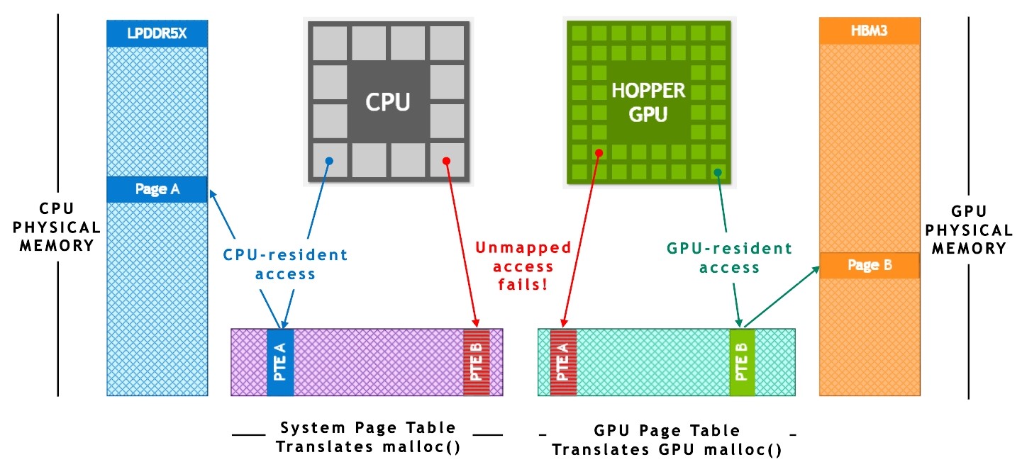
In NVIDIA Grace Hopper Superchip-based systems, ATS enables the CPU and GPU to share a single per-process page table, enabling all CPU and GPU threads to access all system-allocated memory, which can reside on physical CPU or GPU memory. The CPU heap, CPU thread stack, global variables, memory-mapped files, and interprocess memory are accessible to all CPU and GPU threads.
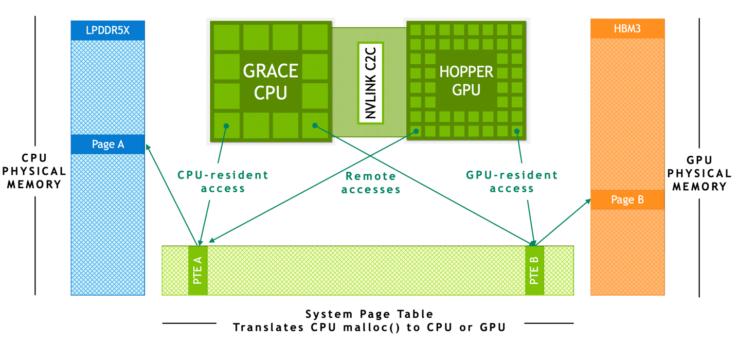
NVIDIA NVLink-C2C hardware-coherency enables the Grace CPU to cache GPU memory at cache-line granularity and for the GPU and CPU to access each other’s memory without page-migrations.
NVLink-C2C also accelerates all atomic operations supported by the CPU and GPU on system-allocated memory. Scoped atomic operations are fully supported and enable fine-grained and scalable synchronization across all threads in the system.
The runtime backs system-allocated memory with physical memory on first touch, either on LPDDR5X or HBM3, depending on whether a CPU or a GPU thread accesses it first. From an OS perspective, the Grace CPU and Hopper GPU are just two separate NUMA nodes. System-allocated memory is migratable so the runtime can change its physical memory backing to improve application performance or deal with memory pressure.
For PCIe-based platforms such as x86 or Arm, you can use the same Unified Memory programming model as the NVIDIA Grace Hopper model. That will eventually be possible through the Heterogeneous Memory Management (HMM) feature, which is a combination of Linux kernel features and NVIDIA driver features that use software to emulate memory coherence between CPUs and GPUs.
On NVIDIA Grace Hopper, these applications transparently benefit from the higher-bandwidth, lower-latency, higher atomic throughput, and hardware acceleration for memory coherency provided by NVLink-C2C, without any software changes.
Superchip architectural features
Here’s a look at the main innovations of the NVIDIA Grace Hopper architecture:
- NVIDIA Grace CPU
- NVIDIA Hopper GPU
- NVLink-C2C
- NVLink Switch System
- Extended GPU memory
NVIDIA Grace CPU
As the parallel compute capabilities of GPUs continue to triple every generation, a fast and efficient CPU is critical to prevent the serial and CPU-only fractions of modern workloads from dominating performance.
NVIDIA Grace CPU is the first NVIDIA data center CPU, and it is built from the ground up to create HPC and AI superchips. Grace provides up to 72 Arm Neoverse V2 CPU cores with the Armv9.0-A ISA, and 4×128-bit wide SIMD units per core with support for Arm’s Scalable Vector Extensions 2 (SVE2) SIMD instruction set.
NVIDIA Grace delivers leading per-thread performance, while providing higher energy efficiency than traditional CPUs. The 72 CPU cores deliver up to a 370 (estimated) score on SPECrate 2017_int_base, ensuring high-performance to satisfy the demands of both HPC and AI heterogeneous workloads.
Modern GPU workloads in machine learning and data science need access to huge amounts of memory. Typically, these workloads would have to use multiple GPUs to store the dataset in HBM memory.
The NVIDIA Grace CPU provides up to 512 GB of LPDDR5X memory, which delivers the optimal balance between memory capacity, energy efficiency, and performance. It supplies up to 546 GB/s of LPDDR5X memory bandwidth, which NVLink-C2C makes accessible to the GPU at 900 GB/s total bandwidth.
A single NVIDIA Grace Hopper Superchip provides the Hopper GPU with a total of 608 GB of fast-accessible memory, almost the total amount of slow memory available in a DGX-A100-80; an eight-GPU system of the previous generation.
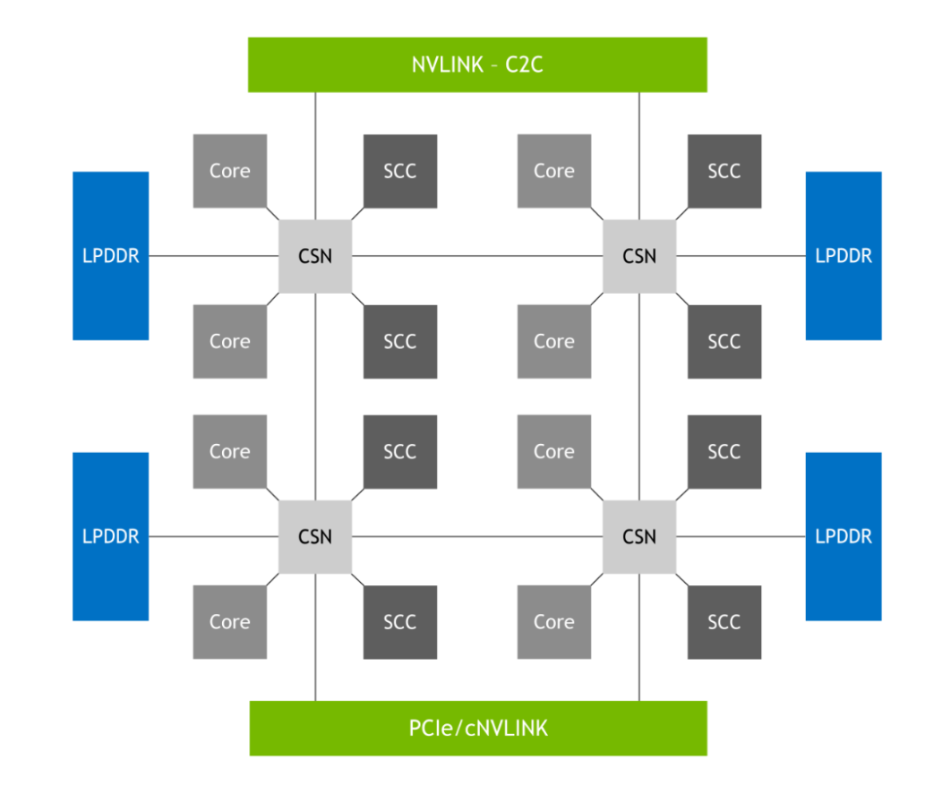
This is made possible by the NVIDIA SCF shown in Figure 7, a mesh fabric and distributed cache that provides up to 3.2 TB/s of total bisection bandwidth to realize the full performance of CPU cores, memory, system I/Os, and NVLink-C2C. The CPU cores and SCF Cache partitions (SCCs) are distributed throughout the mesh, while Cache Switch Nodes (CSNs) route data through the fabric and serve as interfaces between the CPU cores, cache memory, and the rest of the system.
NVIDIA Hopper GPU
The NVIDIA Hopper GPU is the ninth-generation NVIDIA data center GPU. It is designed to deliver orders-of-magnitude improvements for large-scale AI and HPC applications compared to previous NVIDIA Ampere GPU generations. The Hopper GPU also features multiple innovations:
- New fourth-generation Tensor Cores perform faster matrix computations than ever before on an even broader array of AI and HPC tasks.
- A new transformer engine enables H100 to deliver up to 9x faster AI training and up to 30x faster AI inference speedups on large language models compared to the prior generation NVIDIA A100 GPU.
- Improved features for spatial and temporal data locality and asynchronous execution enable applications to always keep all units busy and maximize power efficiency.
- Secure Multi-Instance GPU (MIG) partitions the GPU into isolated, right-sized instances to maximize quality of service (QoS) for smaller workloads.
NVIDIA Hopper is the first truly asynchronous GPU. Its Tensor Memory Accelerator (TMA) and asynchronous transaction barrier enable threads to overlap and pipeline independent data movement and data processing, enabling applications to fully utilize all units.
New spatial and temporal locality features like thread block clusters, distributed shared memory, and thread block reconfiguration provide applications with fast access to larger amounts of shared memory and tools. This enables applications to better reuse data while it’s on-chip, further improving application performance.
For more information, see NVIDIA H100 Tensor Core Architecture Overview and NVIDIA Hopper Architecture In-Depth.
NVLink-C2C: A high-bandwidth, chip-to-chip interconnect for superchips
NVIDIA Grace Hopper fuses an NVIDIA Grace CPU and NVIDIA Hopper GPU into a single superchip through the NVIDIA NVLink-C2C, a 900 GB/s chip-to-chip coherent interconnect that enables programming the Grace Hopper Superchip with a unified programming model.
The NVLink Chip-2-Chip (C2C) interconnect provides a high-bandwidth direct connection between a Grace CPU and a Hopper GPU to create the Grace Hopper Superchip, which is designed for drop-in acceleration of AI and HPC applications.
With 900 GB/s of bidirectional bandwidth, NVLink-C2C provides 7x the bandwidth of x16 PCIe Gen links at lower latency. NVLink-C2C also only uses 1.3 picojoules per bit transferred, which is greater than 5x more energy-efficient than PCIe Gen 5.
Furthermore, NVLink-C2C is a coherent memory interconnect with native hardware support for system-wide atomic operations. This improves the performance of memory accesses to non-local memory, such as CPU and GPU threads accessing memory resident in the other device. Hardware coherency also improves the performance of synchronization primitives, reducing the time the GPU or CPU wait on each other and increasing total system utilization.
Finally, hardware coherency also simplifies the development of heterogeneous computing applications using popular programming languages and frameworks. For more information, see the NVIDIA Grace Hopper Programming Model section.
NVLink Switch System
The NVIDIA NVLink Switch System combines fourth-generation NVIDIA NVLink technology with the new third-generation NVIDIA NVSwitch. A single level of the NVSwitch connects up to eight Grace Hopper Superchips, and a second level in a fat-tree topology enables networking up to 256 Grace Hopper Superchips with NVLink. A Grace Hopper Superchip pair exchanges data at up to 900 GB/s.
With up to 256 Grace Hopper Superchips, the network delivers up to 115.2 TB/s all-to-all bandwidth. This is 9x the all-to-all bandwidth of the NVIDIA InfiniBand NDR400.
The fourth-generation NVIDIA NVLink technology enables GPU threads to address up to 150 TB of memory provided by all superchips in the NVLink network using normal memory operations, atomic operations, and bulk transfers. Communication libraries like MPI, NCCL, or NVSHMEM transparently leverage the NVLink Switch System when available.
Extended GPU memory
The NVIDIA Grace Hopper Superchip is designed to accelerate applications with exceptionally large memory footprints, larger than the capacity of the HBM3 and LPDDR5X memory of a single superchip. For more information, see the NVIDIA Grace Hopper Accelerated Applications section.
The Extended GPU Memory (EGM) feature over the high-bandwidth NVLink-C2C enables GPUs to access all the system memory efficiently. EGM provides up to 150 TBs of system memory in a multi-node NVSwitch-connected system. With EGM, physical memory can be allocated to be accessible from any GPU thread in the multi-node system. All GPUs can access EGM at the minimum of GPU-GPU NVLink or NVLink-C2C speed.
Memory accesses within a Grace Hopper Superchip configuration go through the local high-bandwidth NVLink-C2C at 900 GB/s total. Remote memory accesses are performed through GPU NVLink and, depending on the memory being accessed, also NVLink-C2C (Figure 11). With EGM, GPU threads can now access all memory resources available over the NVSwitch fabric, both LPDDR5X and HBM3, at 450 GB/s.

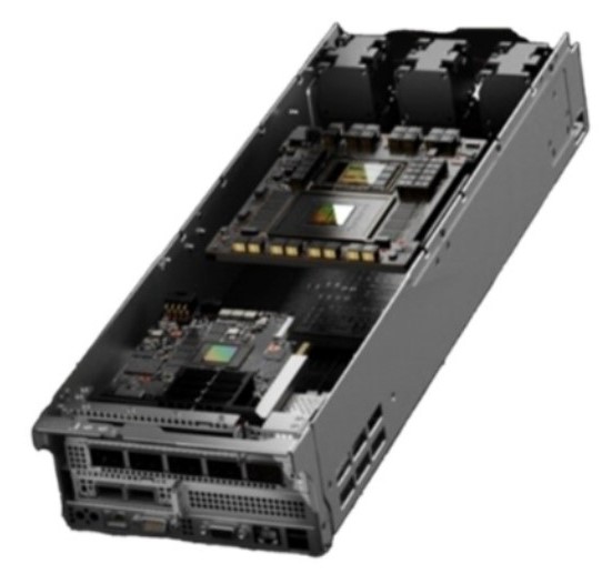
NVIDIA HGX Grace Hopper
NVIDIA HGX Grace Hopper has a single Grace Hopper Superchip per node, paired with BlueField-3 NICs or OEM-Defined I/O and optionally an NVLink Switch System. It can be air– or liquid-cooled and has up to 1,000W TDP.
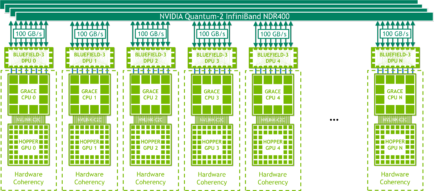
NVIDIA HGX Grace Hopper with InfiniBand
NVIDIA HGX Grace Hopper with Infiniband (Figure 13) is ideal for the scale-out of traditional machine learning (ML) and HPC workloads that are not bottlenecked by network communication overheads of InfiniBand, which is one of the fastest interconnects available.
Each node contains one Grace Hopper Superchip and one or more PCIe devices like NVMe solid-state drives and BlueField-3 DPUs, NVIDIA ConnectX-7 NICs, or OEM-defined I/O. With 16x PCIe Gen 5 lanes, an NDR400 InfiniBand NIC provides up to 100 GB/s of total bandwidth across the superchips. Combined with NVIDIA BlueField-3 DPUs, this platform is easy to manage and deploy and uses a traditional HPC and AI cluster networking architecture.
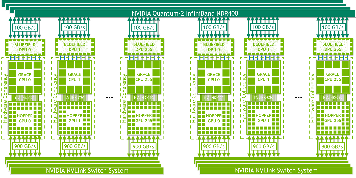
NVIDIA HGX Grace Hopper with NVLink Switch
NVIDIA HGX Grace Hopper with NVLink Switch is ideal for strong scaling giant machine learning and HPC workloads. It enables all GPU threads in the NVLink-connected domain to address up to 150 TB of memory at up to 900 GB/s total bandwidth per superchip in a 256-GPU NVLink-connected system. The a simple programming model uses pointer load, store, and atomic operations. Its 450 GB/s all-reduce bandwidth and up to 115.2 TB/s bisection bandwidth make this platform ideal for strong-scaling the world’s largest and most challenging AI training and HPC workloads.
NVLink-connected domains are networked with NVIDIA InfiniBand networking, for example, NVIDIA ConnectX-7 NICs or NVIDIA BlueField-3 data processing units (DPUs) paired with NVIDIA Quantum 2 NDR switches or OEM-defined I/O solutions.
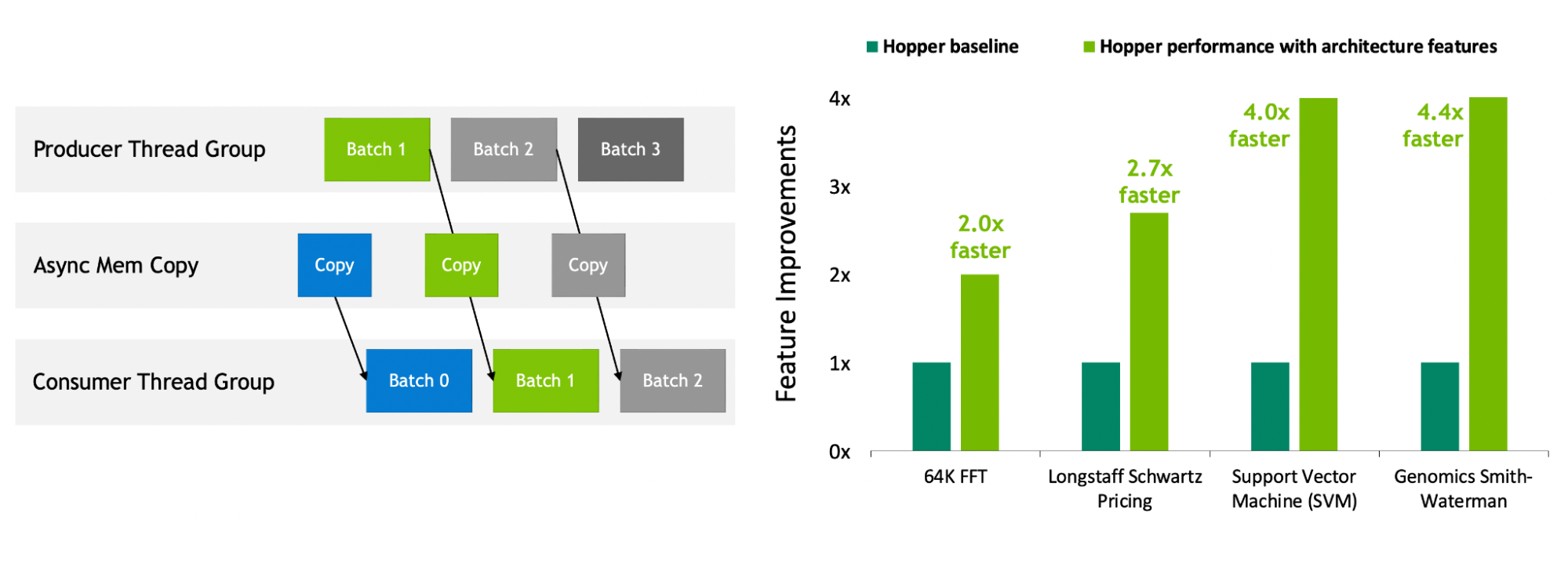
Delivering performance breakthroughs
The NVIDIA Grace Hopper Superchip Architecture whitepaper expands on the details covered in this post. It walks you through how Grace Hopper delivers the performance breakthroughs shown on Figure 1 over what is currently the most powerful PCIe-based accelerated platforms powered by NVIDIA Hopper H100 PCIe GPUs.
Do you have any applications that would be perfect for the NVIDIA Grace Hopper Superchip? Let us know in the comments!
Acknowledgments
We would like to thank Jack Choquette, Ronny Krashinsky, John Hubbard, Mark Hummel, Greg Palmer, Ryan Wells, Alex Ishii, Jonah Alben, and the many NVIDIA architects and engineers who contributed to this post.
