
The NVIDIA Grace CPU is the first data center CPU developed by NVIDIA. Combining NVIDIA expertise with Arm processors, on-chip fabrics, system-on-chip (SoC) design, and resilient high-bandwidth low-power memory technologies, the Grace CPU was built from the ground up to create the world’s first superchip for computing. At the heart of the superchip, lies the NVLink Chip-2-Chip (C2C). The NVLink-C2C enables the NVIDIA Grace CPU to communicate at 900 GB/s bidirectional bandwidth with another NVIDIA Grace CPU or the NVIDIA Hopper GPU in the superchip.
The NVIDIA Grace Hopper Superchip pairs a power-efficient, high-bandwidth NVIDIA Grace CPU with a powerful NVIDIA H100 Hopper GPU using NVLink-C2C to maximize the capabilities for strong-scaling high-performance computing (HPC) and giant AI workloads. More information is available in the NVIDIA Grace Hopper Superchip whitepaper.
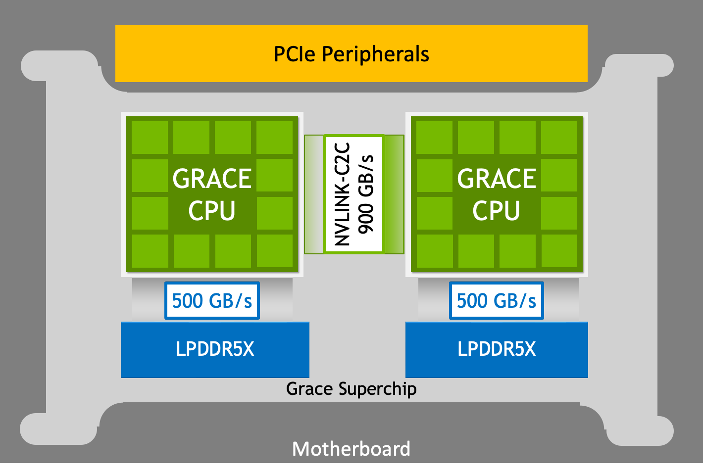
The NVIDIA Grace CPU Superchip is built using two NVIDIA Grace CPUs connected using NVLink-C2C. The superchip builds on the existing Arm ecosystem to create the first no-compromise Arm CPU for HPC, demanding cloud workloads, and high-performance and power-efficient dense infrastructure.
In this post, you will learn about the NVIDIA Grace CPU Superchip and the technologies that deliver the performance and power efficiency of the NVIDIA Grace CPU. See the NVIDIA Grace CPU Superchip Architecture whitepaper for more information.
A superchip built for HPC and AI workloads
The NVIDIA Grace CPU Superchip represents a revolution in compute platform design. This superchip integrates the performance of a two-socket x86-64 server or workstation into a single chip. This enables a more effective and efficient computing platform with 2x the compute density at lower power envelopes.
| NVIDIA Grace CPU Superchip architecture features | |
| Core architecture | Neoverse V2 Cores: Armv9 with 4x128b SVE2 |
| Core count | 144 |
| Cache | L1: 64 KB I-cache + 64 KB D-cache per core L2: 1 MB per core L3: 234 MB per superchip |
| Memory technology | LPDDR5X with ECC, co-packaged |
| Raw memory BW | Up to 1 TB/s |
| Memory size | Up to 960 GB |
| FP64 peak | 7.1 TFLOPS |
| PCIe | 8x PCIe Gen 5 x16 interfaces; option to bifurcate total 1 TB/s PCIe bandwidth. Additional low-speed PCIe connectivity for management. |
| Power | 500 W TDP with memory, 12 V supply |
The NVIDIA Grace CPU was designed to deliver high single-threaded performance, high memory bandwidth, and outstanding data movement capabilities with leadership performance per watt. The NVIDIA Grace CPU Superchip combines two NVIDIA Grace CPUs connected over 900 GB/s bidirectional bandwidth NVLink-C2C. It delivers 144 Arm Neoverse V2 cores with up to 1 TB/s bandwidth of data center class LPDDR5X memory with error correction code (ECC) memory.
Alleviate bottlenecks with NVLink-C2C interconnect
To scale up to 144 Arm Neoverse V2 cores and move data between both CPUs, the NVIDIA Grace CPU Superchip needed a high-bandwidth connection between the CPUs. The NVLink C2C interconnect provides a high-bandwidth direct connection between two NVIDIA Grace CPUs to create the NVIDIA Grace CPU Superchip.
Scale cores and bandwidth with NVIDIA Scalable Coherency Fabric
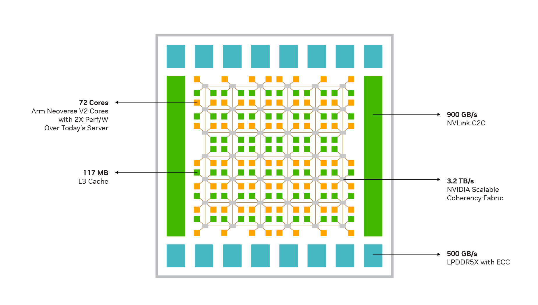
Modern CPU workloads require fast data movement. Designed by NVIDIA, Scalable Coherency Fabric (SCF) is a mesh fabric and distributed cache architecture designed to scale cores and bandwidth (Figure 3). SCF provides over 3.2 TB/s of total bisection bandwidth to keep data flowing between the CPU cores, NVLink-C2C, memory, and system I/O.
The CPU cores and SCF cache partitions are distributed throughout the mesh, while Cache Switch Nodes (CSNs) route data through the fabric and serve as interfaces between the CPU, cache memory, and system I/Os. An NVIDIA Grace CPU Superchip has 234 MB of distributed L3 cache across the two chips.
LPDDR5X
Power efficiency and memory bandwidth are both critical components of data center CPUs. The NVIDIA Grace CPU Superchip uses up to 960 GB of server-class low-power DDR5X (LPDDR5X) memory with ECC. This design strikes the optimal balance of bandwidth, energy efficiency, capacity, and cost for large-scale AI and HPC workloads.
Compared to an eight-channel DDR5 design, the NVIDIA Grace CPU LPDDR5X memory subsystem provides up to 53% more bandwidth at one-eighth the power per gigabyte per second while being similar in cost. An HBM2e memory subsystem would have provided substantial memory bandwidth and good energy efficiency but at more than 3x the cost-per-gigabyte and only one-eighth the maximum capacity available with LPDDR5X.
The lower power consumption of LPDDR5X reduces the overall system power requirements and enables more resources to be put toward CPU cores. The compact form factor enables 2x the density of a typical DIMM-based design.
NVIDIA Grace CPU I/O
The NVIDIA Grace CPU Superchip supports up to 128 lanes of PCIe Gen 5 for I/O connectivity. Each of the 8 PCIe Gen 5 x16 links supports up to 128 GB/s of bidirectional bandwidth. It can be bifurcated into 2x8s for additional connectivity and supports a variety of PCIe slot form factors. It has out-of-the-box support for NVIDIA GPUs and NVIDIA DPUs, NVIDIA ConnectX SmartNICs, E1.S and M.2 NVMe devices, and modular BMC options.
NVIDIA Grace CPU core architecture
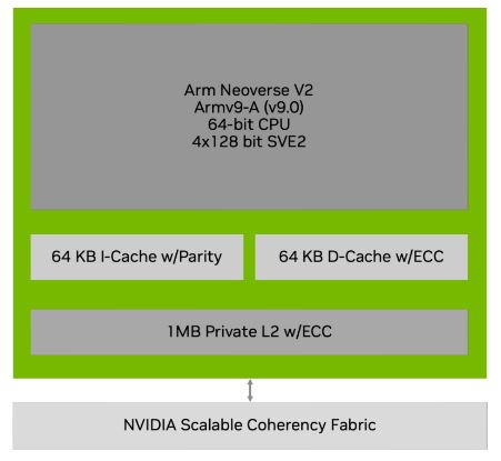
To enable maximum workload acceleration, a fast and efficient CPU is an important component for system design. At the heart of the NVIDIA Grace CPU are the Arm Neoverse V2 CPU cores. Neoverse V2 is the latest in the Arm V-series of infrastructure CPU cores, which are optimized to deliver leading performance per thread while at the same time providing top energy efficiency compared to traditional CPUs.
Arm architecture
The NVIDIA Grace CPU Neoverse V2 core implements the Armv9-A architecture, which extends the architecture defined in the Armv8-A architectures up to Armv8.5-A. Any application binaries built for an Armv8 architecture up to Armv8.5-A will execute on the NVIDIA Grace CPU. That includes binaries targeting CPUs like the Ampere Altra, AWS Graviton2, and AWS Graviton3.
SIMD instructions
The Neoverse V2 implements two single instruction multiple data (SIMD) vector instruction sets in a 4×128-bit configuration: the Scalable Vector Extension version 2 (SVE2), and Advanced SIMD (NEON). Each of the four 128-bit functional units can retire either SVE2 or NEON instructions. This design enables more codes to take full advantage of SIMD performance. SVE2 further extends the SVE ISA with advanced instructions that can accelerate key HPC applications like machine learning, genomics, and cryptography.
Atomic operation
The NVIDIA Grace CPU supports the Large System Extension (LSE) which was first introduced in Armv8.1. LSE provides low-cost atomic operations, which can improve system throughput for CPU-to-CPU communication, locks, and mutexes. These instructions can operate on integer data. All compilers supporting the NVIDIA Grace CPU use these instructions automatically in synchronization functions like the GNU Compiler Collection __atomic built-ins and std::atomic. The improvement can be up to an order of magnitude when using LSE atomics instead of load/store exclusives.
Armv9 additional features
The NVIDIA Grace CPU implements multiple key features of the Armv9 portfolio that provide utility in general-purpose data center CPUs. This includes cryptographic acceleration, scalable profiling extension, virtualization extensions, full memory encryption, secure boot, and more.
NVIDIA Grace CPU software
The NVIDIA Grace CPU Superchip is built to provide software developers with a standards-compliant platform.
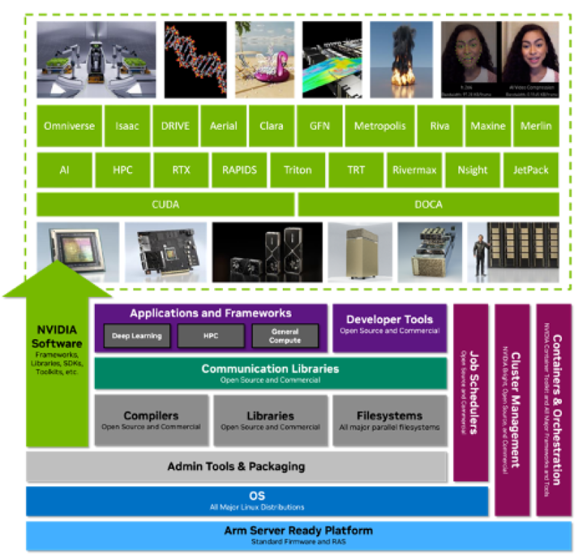
The NVIDIA Grace CPU complies with the Arm Server Base System Architecture (SBSA) to enable standards-compliant hardware and software interfaces. In addition, to enable standard boot flows on NVIDIA Grace CPU-based systems, the NVIDIA Grace CPU has been designed to support Arm Server Base Boot Requirements (SBBR). All major Linux distributions, and the vast collections of software packages that they provide, work perfectly and without modification on the NVIDIA Grace CPU.
Compilers, libraries, tools, profilers, system administration utilities, and frameworks for containerization and virtualization are available today and can be used on the NVIDIA Grace CPU the same as any other data center CPU.
In addition, the entire NVIDIA software stack is available for the NVIDIA Grace CPU. The NVIDIA HPC SDK and every NVIDIA CUDA component has Arm-native installers and containers. The NVIDIA GPU Cloud (NGC) also provides deep learning, machine learning, and HPC containers optimized for Arm. The NVIDIA Grace CPU follows mainstream CPU design principles and is programmed just like any other server CPU.
Delivering performance efficiency
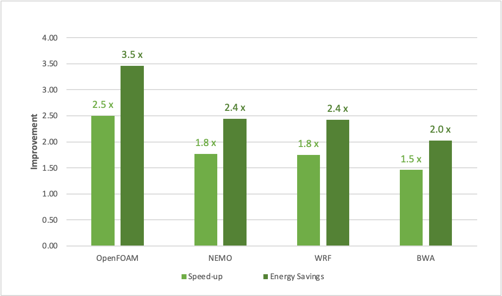
The NVIDIA Grace Superchip Architecture whitepaper expands on the details covered in this post. It provides an in-depth explanation of how the NVIDIA Grace CPU delivers the superior performance shown in Figure 1, as well as the technological innovations behind the performance.
Acknowledgments
Thank you Thomas Bradley, Jonah Alben, Brian Kelleher, Nick Stam, Jasjit Singh, Anurag Chaudhary, Giridhar Chukkapalli, Soumya Shyamasundar, Ian Karlin, Suryakant Patidar, Alejandro Chacon, Matthew Nicely, Steve Scalpone, Polychronis Xekalakis, and many other NVIDIA architects and engineers who contributed to this post.