
In 3GPP fifth generation (5G) cellular standard, layer 1 (L1) or the physical layer (PHY) is the most compute-intensive part of the radio access network (RAN) workload. It involves some of the most complex mathematical operations with sophisticated algorithms like channel estimation and equalization, modulation/demodulation, and forward error correction (FEC). These functions require high compute densities to maintain 5G’s low latency requirements and signal integrity in different radio conditions.
Traditionally, this layer has been implemented using purpose-built hardware, for example, specialized application-specific integrated circuits (ASICs) with digital signal processing (DSP) cores. This approach, has several drawbacks, however, namely an inability to scale performance, tight hardware-software coupling, and closed single vendor solution. This all results in the high cost of deploying and operating the RAN.
To address these challenges, the industry has been evolving towards virtualized RAN (vRAN) and open RAN (O-RAN) architectures using x86 CPU-based commercial-off-the-shelf (COTS) servers. There’s an expectation that this will lower the cost, and that the resultant hardware-software disaggregation will drive faster innovation cycles, leading the path toward a cloud-native architecture.
However, the complex signal processing needs of L1 make it difficult to achieve the desired vRAN performance on x86 CPU-based COTS servers. To address this L1 performance gap, some industry players are building fixed-function accelerators. Examples include discrete ASICs, field programmable gate arrays (FPGAs), or integrated system-on-chips (SoCs).
Fixed-function accelerators supplement the CPU performance and accelerate the processing of a selected set of functions offloaded from a vRAN L1 pipeline, while retaining the majority of the L1 processing within the CPU. This is an acceleration approach dubbed in the industry as lookaside acceleration.
In many ways, fixed-function lookaside accelerator-based vRAN platforms are akin to going back in time to the appliance-like, macro base station architecture models, which lack scalability and agility. What our industry needs is a fully software-defined vRAN that can deliver programmability, performance, and software scalability while supporting interoperability and multi-vendor solutions, a key tenet of O-RAN.
With the emergence of artificial intelligence and machine learning (AI/ML) as one of the key driving forces shaping the landscape beyond 5G, it is equally important for the industry to embrace a vRAN platform that is future-proof. It should be ready to enable new capabilities like AI/ML as augmented features on top of the existing RAN infrastructure.
NVIDIA Aerial platform
The NVIDIA Aerial platform brings together the NVIDIA Aerial vRAN stack for 5G, AI frameworks, and the accelerated compute infrastructure. It delivers the key virtues by using the high degree of programmability and parallel processing capabilities of GPUs. The platform differs from the traditional fixed-function lookaside acceleration approach in two ways:
- It does not use any fixed-function accelerator
- Instead of selectively offloading a subset of L1 functions to the accelerator, NVIDIA Aerial implements the entire L1 processing pipeline within GPU, an approach called inline acceleration.
The NVIDIA Aerial vRAN stack is a fully programmable, software-defined, AI-capable, and cloud-native 5G vRAN. For more information about how NVIDIA Aerial got started, see the NVIDIA cuBB GPU Accelerated 5G vRAN session from the 2019 Mobile World Congress.
Our goal with this post is to show the merits of NVIDIA Aerial, a GPU-based inline architecture. We explain why programmable, inline acceleration is a critical foundation to deliver high-performance, energy-efficient, scalable, and cloud-native vRAN.
Understanding the lookaside and inline acceleration models
To begin with, look into the generic working principles of the lookaside and Inline acceleration models.
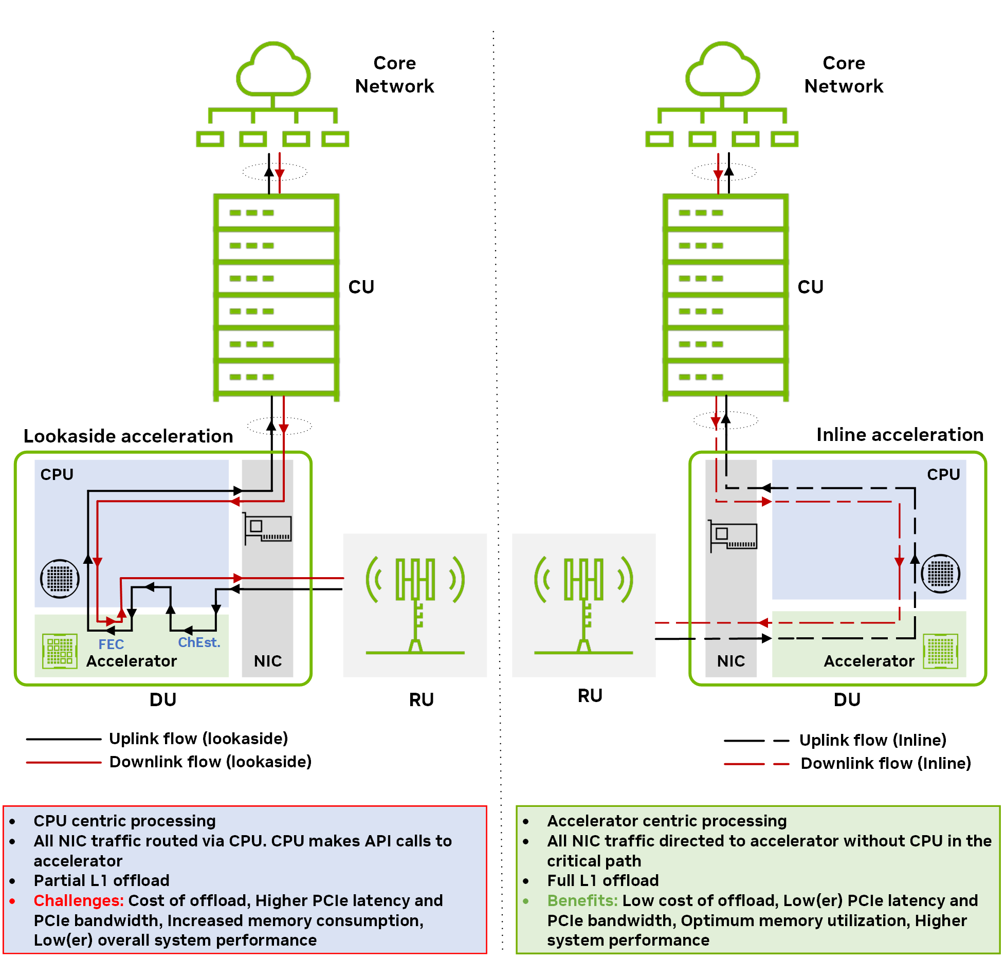
Figure 1 shows the data flow in downlink and uplink directions for two different acceleration models: Lookaside and Inline. For more information, see Hardware Acceleration for Open Radio Access Networks: A Contemporary Overview.
In a lookaside acceleration model, the host CPU invokes data processing offload to the accelerator and receives the results back when the processing is done. The lookaside approach requires a back-and-forth data transfer between the CPU and the accelerator. If there are multiple, non-contiguous functional blocks offload (for example, FEC decode and channel estimation), the overhead of the host-to-device data transfer and resulting memory bandwidth consumption becomes significantly high.
In an inline acceleration model, the accelerator directly exchanges data with the network interface card (NIC) without involving the CPU in the critical path. For full L1 acceleration in an inline model, the entire L1 processing is offloaded to the accelerator.
Inline acceleration does not require a back-and-forth redundant data transfer between the host and the device, unlike lookaside acceleration. The net effect of this is more efficient usage of memory and PCIe bandwidth.
Programmable, inline acceleration is better for vRAN
Take a closer look at vRAN solutions based on two acceleration approaches:
- Lookaside with a fixed-function accelerator
- Inline with a programmable accelerator
In this section, we highlight the merits and limitations of each and explain why the inline approach with programmable accelerators is more suitable for vRAN compared to lookaside with fixed-function accelerators.
- Lookaside offload costs affect latency and performance
- Lookaside quality of service guarantees increase complexity
- Lookaside accelerator integrated as a PCIe device is not equivalent to an inline accelerator
- Fixed-function acceleration is inherently not cloud-native
- Fixed-function accelerators lack scalability
- Fixed-function accelerators are not agile
Lookaside offload costs affect latency and performance
Lookaside acceleration results in a cost of offload due to the request/response transaction across the PCIe interface between the CPU and the accelerator. In the case of multiple, back-and-forth transactions (due to offloading a set of non-contiguous functions), lookaside acceleration increases both the CPU cycle consumption and latency, impacting perf/Watt and perf/$$.
To reduce the cost of offload, the accelerator driver may combine or batch several requests together. However, this leads to undesired buffering and queuing, resulting in significantly higher latency for various user data flows.
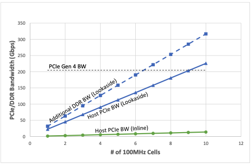
Figure 2 shows the expected host PCIe and the double data rate bandwidth (DDR BW) consumption (Gbps) as the number of supported 4-transmit-4-receive (4T4R) 100MHz cells increases. The graph shows that the aggregated transaction bandwidth needed to support four downlink (DL) layers and two uplink (UL) layers (for each 100MHz cell) when deploying with a lookaside accelerator is much worse. Approximately 40x more bandwidth is consumed when compared to the inline accelerator.
It is also worth mentioning that as the number of cells increases, PCIe Gen4 technology cannot sustain the required bandwidth and PCIe Gen5 technology is required to support the lookaside accelerator.
Lookaside quality of service guarantees increase complexity
Fine-grained QoS support for various user data flows is another challenge with lookaside accelerators. The complex queuing architecture required across the PCIe interface to meet the QoS needs can result in performance degradation and impact tail latency of queued requests to the accelerator.
As an example, consider a DU system that supports mixed user data flows for voice over Internet protocol (VoIP), Internet of things (IoT), enhanced mobile broadband (eMBB), and ultra-reliable low-latency communications (URLLC) applications. In the lookaside model, if a VoIP or URLLC packet gets stuck behind large blocks of eMBB data queued to the accelerator, it incurs significant latency and jitter and degrades the QoS. The fact that this can accumulate over time as every transaction needs to go through a Lookaside accelerator results in significant performance degradation.
There are ways to address these issues through QoS guarantees and hierarchical scheduling across the lookaside PCIe interface. However, this increases both the hardware and the software complexity, resulting in increased cost and energy consumption, as well as reduced cell capacity.
To further demonstrate the cell capacity and power efficiency benefits of deploying an inline accelerator compared to lookaside, we evaluated the performance of both acceleration modes with respect to two metrics for the following system configuration: 100 MHz, 4T4R, 4 DL/2 UL layers:
- Number of 100MHz cells supported
- MHz*Layers/Watt
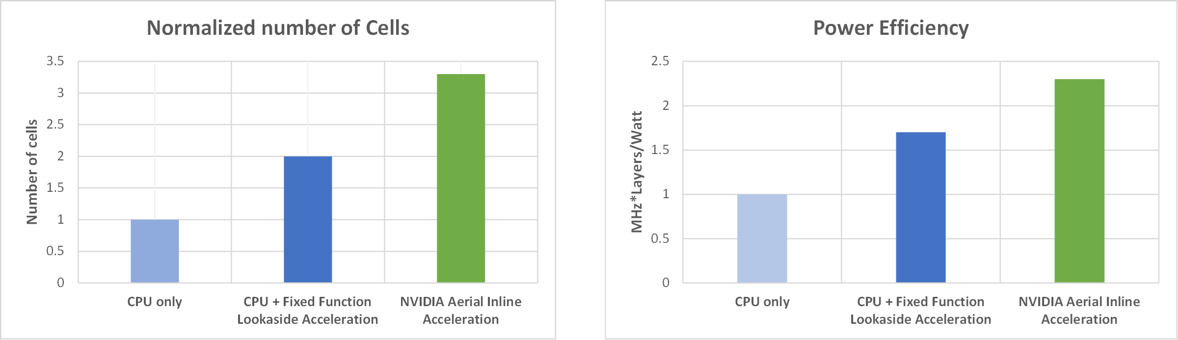
Figure 3 shows the performance comparison, with the number of supported cells metric (normalized) displayed on the left and the MHz*Layers/Watt metric displayed on the right. For each metric, the cell capacity and power efficiency benefits are clear when deploying an inline accelerator, compared to a fixed-function lookaside accelerator or no accelerator (that is, CPU only).
Lookaside accelerator integrated as a PCIe device is not equivalent to an inline accelerator
Some argue that the integration of lookaside accelerators in the CPU makes it an inline architecture. Nothing could be farthest from the truth.
While integration may result in limited power optimization and reduce the component price, any fixed-function lookaside accelerator, such as FEC, integrated in the CPU still manifests as a PCIe device and is accessed through DPDK BBDEV. The net effect is that the same inefficiency exists with fixed-function lookaside accelerators, no matter whether they are discrete components, or integrated in the CPU.
In fact, integrating lookaside accelerators introduce a new set of problems: managing specific CPU stock-keeping units (SKUs), juggling feature prioritization, increasing CPU costs, and so on.
Fixed-function acceleration is inherently not cloud-native
The key tenet of cloud computing is that the infrastructure resources can be shared across applications, increasing the utilization, and delivering better economies of scale.
Fixed-function accelerators (such as FPGA-based, low-density parity check (LDPC), SoC-based L1 high-PHY and so on) are single-purpose. When a fixed-function accelerator is not being used by 5G vRAN, it is a wasted resource that is not used by any other application.
Typical 5G networks run at less than 50% average utilization. This means a fixed-function lookaside accelerator can just sit there in the cloud, not being used for more than 50% of the time. On the other hand, a general-purpose and programmable accelerator such as a GPU can be reused for other applications, such as large language model (LLM) training and inferencing, computer vision, and analytics.
Data Plane Development Kit Baseband Device (DPDK BBDEV) is the commonly used application programming interface (API) for lookaside acceleration. It is not well-suited for cloud-native deployments. DPDK has many constructs that were designed for high-performance, in-network appliances, including the following:
- Huge page tables
- Pre-allocated buffers
- Pinned memory
- Single-root input/output virtualization (SR-IOV)
- Queue-centric enqueue-dequeue operations
These features, however, create a strong affinity towards the underlying hardware, not enabling seamless portability and workload movement in a true cloud-native fashion.
Fixed-function accelerators lack scalability
A major drawback of fixed-function accelerators like FEC LDPC, discrete Fourier transform (DFT), inverse DFT (iDFT), and other selected baseband Layer 1 functions is that, while it may be right-sized for one configuration or use case, it is suboptimal for another configuration.
Take FEC LDPC as an example. In a typical 5G frequency range 1 (FR1) sub-6 GHz system with 4T4R antenna and DDDSUUDDDD channel configuration (D: downlink, U: uplink, S: special) and 4 DL/2 UL layers, the LDPC decoder may constitute about 25% of the physical uplink shared channel (PUSCH) workload in an UL slot.
Keeping other configurations unchanged, if the system dimension scales from a 4T4R to 64T64R antenna configuration (massive MIMO), the LDPC decoder compute load on the PUSCH pipeline, as it turns out, does not increase commensurately. In fact, in this higher dimensional system, LDPC constitutes approximately just 10% of the overall uplink workload.
Why does this happen? It’s because the complexity of the LDPC decoder scales only linearly with the number of layers, where other algorithms, such as channel estimation or detection, scale superlinearly. This can easily lead to suboptimal designs from the point of view of resource utilization and power consumption, if these functions are implemented in fixed-function acceleration logic.
Fixed-function accelerators are not agile
Fixed-function accelerators are difficult to evolve with 3GPP releases (for example, with new features) as they are designed for a particular release of the specification. Upgrades of these complex algorithms running on fixed-function accelerators are difficult (especially when implemented in hardware), thereby throttling improvements over time. Also, hardware bug fixes are problematic to resolve, often resulting in costly replacement as being the only viable resolution.
To summarize, fixed-function lookaside acceleration has several drawbacks: an impact on performance and latency, lower energy efficiency, and lack of programmability and scalability. These issues directly result in higher CapEx and OpEx for telco operators.
Next, we discuss an alternate approach taken by NVIDIA, that addresses many of the issues highlighted earlier by harnessing the principles of programmability and inline acceleration. This solution paves the way for industry-leading vRAN.
NVIDIA Aerial: Programmable, GPU-based inline acceleration for vRAN
NVIDIA has taken a thoughtful architectural approach to use the inline architecture for a full L1 offload to a programmable GPU. The architecture uses Bluefield DPUs to bring all fronthaul-enhanced common public radio interface (eCPRI) data traffic into the GPU without the CPU in the data path.
A natural question to ask is why GPUs? The signal processing requirements of the 5G PHY are computationally challenging, compounded by intensive matrix operations. The massive parallelism of the GPU architecture brings the right hardware resources to support this class of workloads.
From a developer perspective, GPUs are programmed using CUDA, the world’s most commercially successful parallel programming framework. This makes your job simpler as you can use mature tools and expansive libraries for software lifecycle management including planning, design, development, optimization, testing, and maintenance. This has been proven by the widespread adoption of GPUs in the computationally complex field of AI and machine learning.
The second question is why inline? Inline architecture provides a full offload of vRAN L1 processing to the GPU without any CPU interactions. The interface for the offload is the functional application platform interface (FAPI), which is an industry standard developed within the Small Cell Forum (SCF). The full offload also avoids the complex and inefficient ping-pong effects of the lookaside model between the CPU and the accelerator across the host PCIe interface, resulting in the improved performance and lower latency explained earlier.
NVIDIA Aerial, enabling fully programmable, cloud-native, AI-capable, and high-performance end-to-end L1 high-PHY (7.2-x split) inline acceleration is built upon two fundamental principles:
- Accelerated compute
- Fast I/O
Accelerated compute is manifested through the component CUDA baseband (cuBB), the software stack providing a GPU-accelerated 5G L1 signal processing pipeline. cuBB delivers unprecedented throughput and efficiency by keeping all PHY layer processing within the high-performance GPU memory. cuBB includes 5G L1 high-PHY acceleration library cuPHY, which is highly optimized for NVIDIA GPUs and offers unparalleled scalability by using a GPU’s massive computing power and high degree of parallelism.
Fast I/O is manifested through the NVIDIA DOCA GPUNetIO module, providing optimized I/O and packet processing by exchanging packets directly between GPU memory and a GPUDirect-capable NVIDIA ConnectX SmartNIC. Enabling fast I/O processing and direct memory access (DMA) technology is essential in unleashing the full potential of inline acceleration.
Towards that goal, the NVIDIA Aerial platform has adopted a GPU-centric approach, implemented with NVIDIA DOCA GPUNetIO Library. In this approach, an NVIDIA GPU directly interacts with an NVIDIA SmartNIC using GPUDirect Async Kernel-initiated Network (GDAKIN) communications to configure and update NIC registers for orchestrating network send and receive operations without the intervention of the CPU. For more information, see Inline GPU Packet Processing with NVIDIA DOCA GPUNetIO.
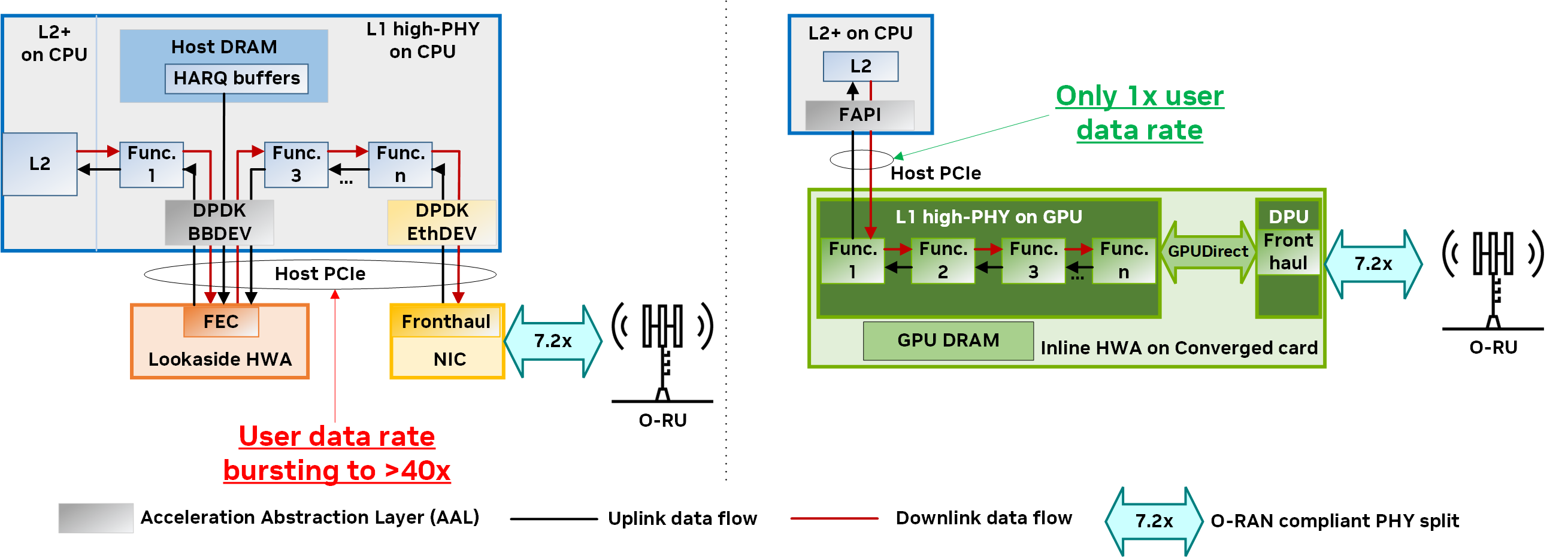
Figure 4 shows the architectural comparison for the PHY layer between the GPU-based inline acceleration implementation using NVIDIA Aerial and the typical fixed-function hardware accelerator (HWA)-based lookaside acceleration. On the right side, the NVIDIA Aerial platform offers a fast, efficient, and streamlined data flow all the way from L2 to L1 and to fronthaul, without requiring CPU staging copies or throttling of the host PCIe bandwidth.
- Higher level acceleration abstraction layer (AAL) between L2 and L1 (that is, FAPI)
- Converged architecture with GPU and DPU
- Interconnect powered by the NVIDIA DOCA GPUNetIO and GPUDirect technologies
As the entire L1 processing pipeline and corresponding data are contained within the GPU kernels and dynamic random-access memory (DRAM) on the same converged card, NVIDIA Aerial does not consume critical shared resources with L2+ (for example, host DRAM or host PCIe), unlike the traditional lookaside architecture (left).
With less CPU core consumption and a high degree of GPU parallelism in processing the entire L1 workload, the NVIDIA Aerial platform delivers a lower CapEx and OpEx solution with unmatched performance, scalability, agility, programmability, and energy efficiency.
NVIDIA Aerial addresses the key requirements
Table 1 presents a snapshot of the key requirements for 5G vRAN, the limitations of the lookaside architecture with a fixed-function accelerator in meeting these requirements, and the benefits of the inline architecture with a GPU-programmable accelerator in addressing those shortcomings.
| Requirements | Fixed-function lookaside architecture | GPU-programmable inline architecture |
| High performance and low latency | Multiple requests and responses across PCIe lead to increased CPU consumption and worse perf/Watt and perf/$$. Higher L1 processing latency due to batching and queuing of lookaside requests. | L2 ↔ L1 ↔ FH streamlined processing pipeline, no back-and-forth transactions over PCIe, leading to better perf/Watt and perf/$$. No buffering/queuing during L1 runtime, resulting in optimal L1 processing latency. |
| Cloud economics | No reuse: only does ‘fixed’ function and not sharable with other applications in cloud infrastructure. | Fully programmable and general purpose resulting in high resource utilization. |
| Application portability | DPDK BBDEV: Not easily portable because of the strong affinity to hardware. | FAPI: Better portability with higher level abstraction between L2 and L1. |
| Scalability | Designed and optimized for a specific system configuration. | Fully programmable and scalable for a range of system configs. |
| Agility | Not programmable, long design cycles, and difficult to update with evolving standards and algorithms. | Fully programmable and software-defined, easy to update for evolving standards and new algorithms. |
Conclusion
In this post, we highlighted the inefficiencies of fixed-function accelerators and the lookaside processing model. We showed you how the lookaside model impacts performance and energy efficiency along with many scalability challenges.
The inline processing model with a programmable accelerator addresses the technical bottlenecks of the fixed-function lookaside acceleration model and delivers high performance, energy efficiency, and scalability across various RAN configurations.
NVIDIA Aerial is the only commercial platform that delivers the key tenets of emerging vRAN: high-performance, software-defined, COTS-based, cloud-native, and AI-ready. It implements the GPU-programmable inline processing model and full L1 offload to deliver efficient performance for a wide range of RAN configurations and use cases with a software architecture that is fully compliant with O-RAN standards.
We invite you to collaborate with us in our quest to modernize the RAN infrastructure and enable an efficient, high-performance, scalable, agile, cloud-native, fully software-defined, and AI-ready vRAN.