
What is the interest in trillion-parameter models? We know many of the use cases today and interest is growing due to the promise of an increased capacity for:
- Natural language processing tasks like translation, question answering, abstraction, and fluency.
- Holding longer-term context and conversational ability.
- Multimodal applications combining language, vision, and speech.
- Creative applications like storytelling, poetry generation, and code generation.
- Scientific applications, such as protein folding predictions and drug discovery.
- Personalization, with the ability to develop a consistent personality and remember user context.
The benefits are great, but training and deploying large models can be computationally expensive and resource-intensive. Computationally efficient, cost-effective, and energy-efficient systems, architected to deliver real-time inference will be critical for widespread deployment. The new NVIDIA GB200 NVL72 is one such system up to the task.
To illustrate, let’s consider the Mixture of Experts (MoE) models. These models help distribute the computational load across multiple experts and train across thousands of GPUs using model parallelism and pipeline parallelism. Making the system more efficient.
However, a new level of parallel compute, high-speed memory, and high-performance communications could enable GPU clusters to make the technical challenge tractable. The NVIDIA GB200 NVL72 rack-scale architecture achieves this goal, which we detail in the following post.
A rack scale design for an exascale AI supercomputer
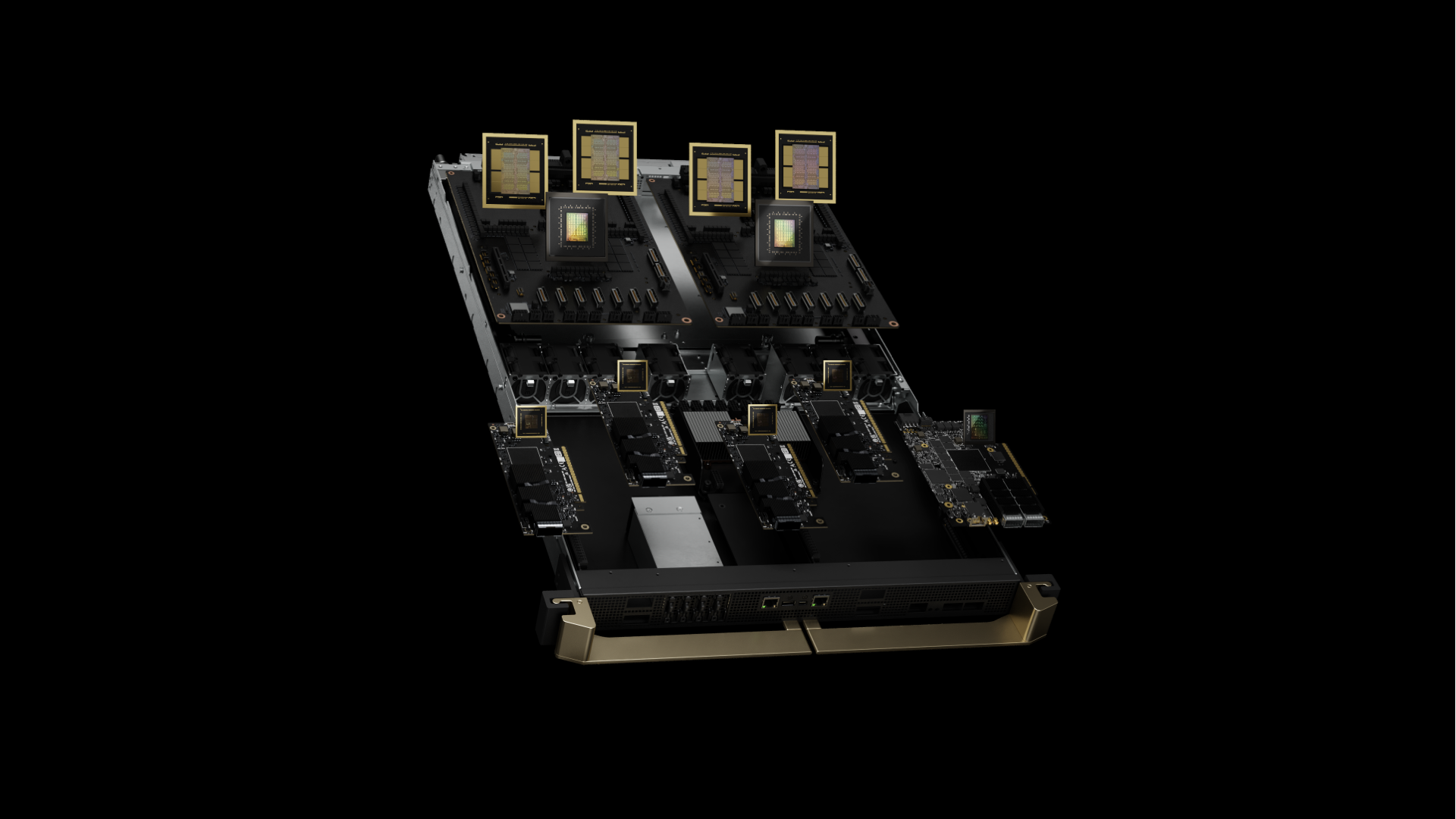
The heart of the GB200 NVL72 is the NVIDIA GB200 Grace Blackwell Superchip. It connects two high-performance NVIDIA Blackwell Tensor Core GPUs and the NVIDIA Grace CPU with the NVLink-Chip-to-Chip (C2C) interface that delivers 900 GB/s of bidirectional bandwidth. With NVLink-C2C, applications have coherent access to a unified memory space. This simplifies programming and supports the larger memory needs of trillion-parameter LLMs, transformer models for multimodal tasks, models for large-scale simulations, and generative models for 3D data.
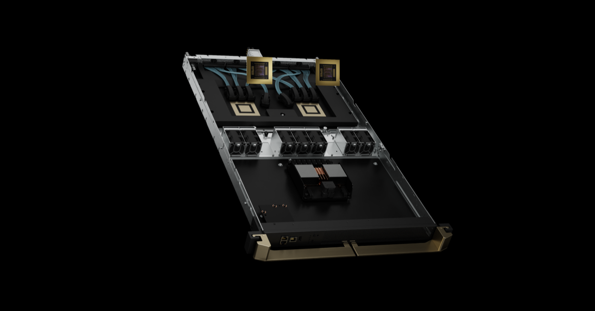
The GB200 compute tray is based on the new NVIDIA MGX design. It contains two Grace CPUs and four Blackwell GPUs. The GB200 has cold plates and connections for liquid cooling, PCIe gen 6 support for high-speed networking, and NVLink connectors for the NVLink cable cartridge. The GB200 compute tray delivers 80 petaflops of AI performance and 1.7 TB of fast memory.
The largest problems require sufficient numbers of groundbreaking Blackwell GPUs to work in parallel efficiently, so they must communicate with high bandwidth and low latency and keep constantly busy.
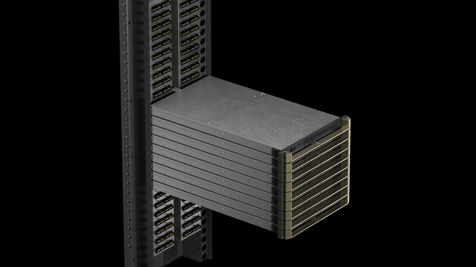
The GB200 NVL72 rack-scale system facilitates parallel model efficiency for the 18 compute nodes using the NVIDIA NVLink Switch System with nine NVLink switch trays, and cable cartridges interconnecting the GPUs and switches.
NVIDIA GB200 NVL36 and NVL72
The GB200 supports 36 and 72 GPUs in NVLink domains. Each rack hosts 18 compute nodes based upon the MGX reference design and the NVLink Switch System. It comes in the GB200 NVL36 configuration with 36 GPUs in one rack and 9 dual GB200 compute nodes. The GB200 NVL72 is configured with 72 GPUs in one rack and 18 dual GB200 compute nodes—or 72 GPUs in two racks with 18 single GB200 compute nodes.
The GB200 NVL72 densely packs and interconnects the GPUs using a copper cable cartridge for operational simplicity. It also uses a liquid cooling system design, delivering 25x lower cost and energy consumption.
Fifth-generation NVLink and NVLink Switch System
The NVIDIA GB200 NVL72 introduces fifth-generation NVLink, which connects up to 576 GPUs in a single NVLink domain with over 1 PB/s total bandwidth and 240 TB of fast memory. Each NVLink switch tray delivers 144 NVLink ports at 100 GB so the nine switches fully connect each of the 18 NVLink ports on every one of the 72 Blackwell GPUs.
The revolutionary 1.8 TB/s of bidirectional throughput per GPU is over 14x the bandwidth of PCIe Gen5, providing seamless high-speed communication for today’s most complex large models.
NVLink over generations
The NVIDIA industry-leading innovation for high-speed low-power SerDes drives the advance of GPU-to-GPU communication, beginning with the introduction of NVLink to accelerate multi-GPU communications at high speed. The NVLink GPU-to-GPU bandwidth is 1.8 TB/s, which is 14x the bandwidth of PCIe. The fifth-generation NVLink is 12x faster than the first generation at 160 GB/s, introduced in 2014. NVLink GPU-to-GPU communications have been instrumental in scaling multi-GPU performance in AI and HPC.
GPU bandwidth advances coupled with the exponential expansion of NVLink domain size have increased the total bandwidth of an NVLink domain 900x since 2014 to 1 PB/s for a 576 Blackwell GPU NVLink domain.
Use cases and performance results
The compute and communications capabilities of the GB200 NVL72 are unprecedented, bringing grand challenges in AI and HPC within practical reach.
AI training
The GB200 includes a faster second-generation transformer engine featuring FP8 precision. It delivers 4X faster training performance with 32k GB200 NVL72 for large language models like GPT-MoE-1.8T compared to the same number of NVIDIA H100 GPUs.
AI inference
The GB200 introduces cutting-edge capabilities and a second-generation transformer engine that accelerates LLM inference workloads. It delivers a 30x speedup for resource-intensive applications like the 1.8T parameter GPT-MoE compared to the previous H100 generation. This advancement is made possible with a new generation of Tensor Cores, which introduce FP4 precision and the many advantages that come with fifth-generation NVLink
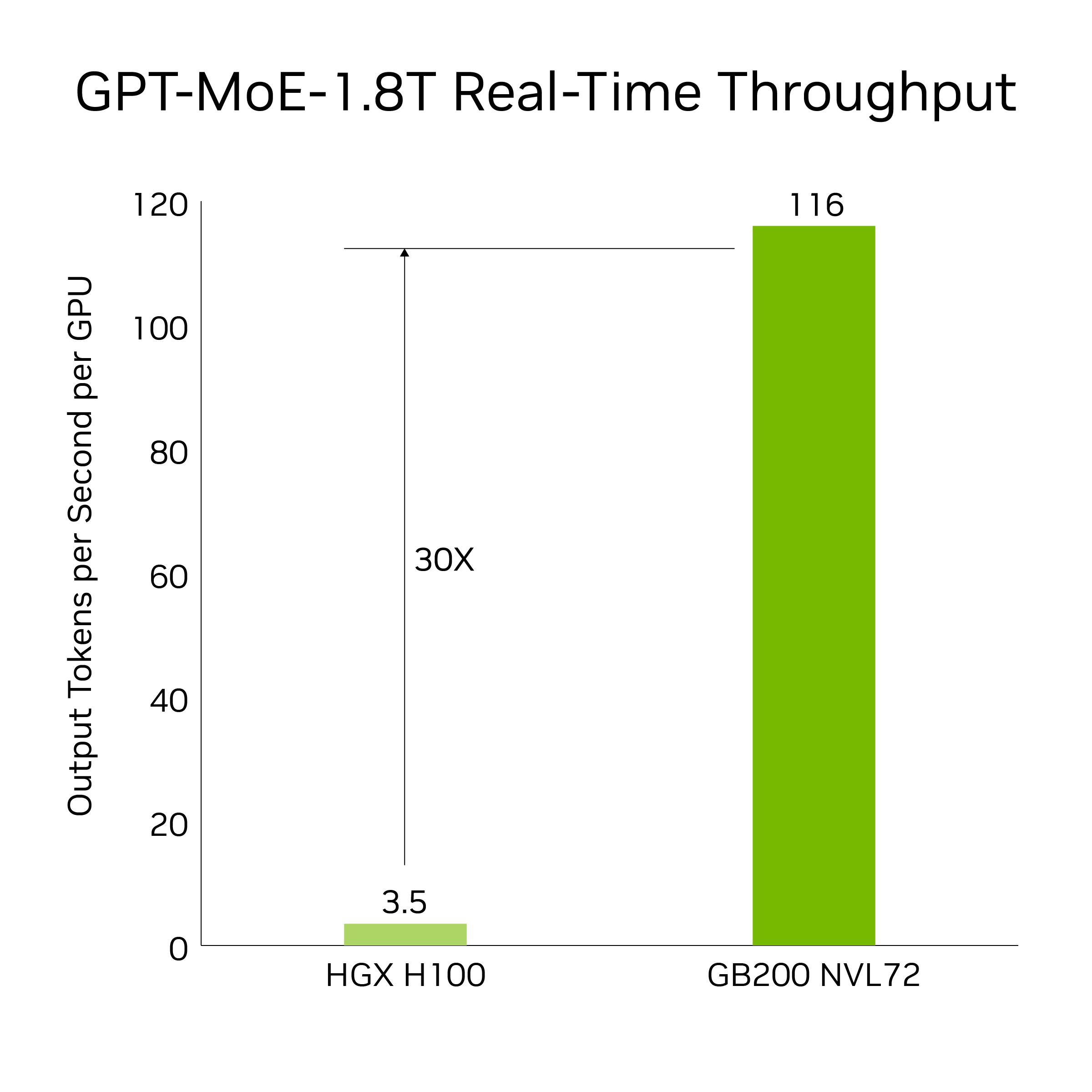
Results based on token-to-token latency = 50 ms; real-time, first token latency = 5,000 ms; input sequence length = 32,768; output sequence length = 1,024 output, 9x eight-way HGX H100 air-cooled: 400 GB IB Network vs 18 GB200 Superchip liquid-cooled: NVL72, per GPU performance comparison. Projected performance is subject to change.
Data processing
Big data analytics helps organizations unlock insights and make better-informed decisions. Organizations continuously generate data at scale and rely on various compression techniques to alleviate bottlenecks and save on storage costs. To process these datasets efficiently on GPUs, the Blackwell architecture introduces a hardware decompression engine that can natively decompress compressed data at scale and speed up analytics pipelines end-to-end. The decompression engine natively supports decompressing data compressed using LZ4, Deflate, and Snappy compression formats.
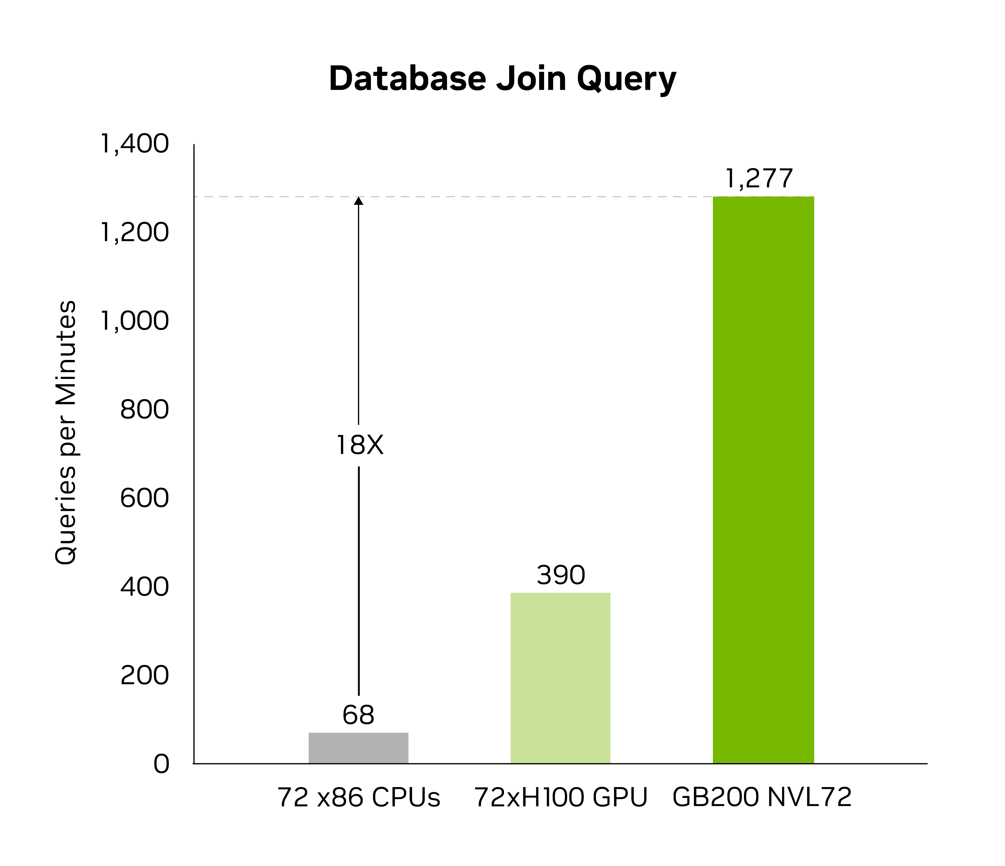
The decompression engine speeds up memory-bound kernel operations. It provides performance up to 800 GB/s and enables Grace Blackwell to perform 18x faster than CPUs (Sapphire Rapids) and 6x faster than NVIDIA H100 Tensor Core GPUs for query benchmarks.
With the blazing 8 TB/s of high memory bandwidth and the Grace CPU high-speed NVlink-Chip-to-Chip (C2C), the engine speeds up the entire process of database queries. This results in top-notch performance across data analytics and data science use cases. This enables organizations to obtain insights quickly while reducing their costs.
Physics-based simulations
Physics-based simulations are still the mainstay of product design and development. From planes and trains to bridges, silicon chips, and even pharmaceuticals, testing and improving products through simulation saves billions of dollars.
Application-specific integrated circuits are designed almost exclusively on CPUs in a long and complex workflow, including analog analysis to identify voltages and currents. The Cadence SpectreX simulator is one example of a solver. SpectreX circuit simulations are projected to run 13x quicker on a GB200 Grace Blackwell Superchip—which connects Blackwell GPUs and Grace CPUs — than on a traditional CPU.

Cadence SpectreX (Spice simulator) | CPU: 16 cores x86 CPU dataset: KeithC Design TSMC N5 | Cadence Fidelity (LES CFD Solver) | CPU: 16 cores x86 CPU Dataset: GearPump 2M cells | Performance projections for GB200 subject to change
Over the last two years, the industry has increasingly turned to GPU-accelerated computational fluid dynamics (CFD) as a key tool. Engineers and equipment designers use it to study and predict the behavior of their designs. Cadence Fidelity runs CFD simulations that are projected as much as 22x faster on GB200 systems than on traditional CPU-powered systems.
We look forward to exploring the possibilities of Cadence Fidelity on the GB200 NVL72. With parallel scalability and 30 TB of memory per rack, we aim to capture flow details that have never been captured before.
Summary
To recap, we reviewed the GB200 NVL72 rack-scale design and, in particular, learned about its unique capability to connect 72 Blackwell GPUs over a single NVIDIA NVLink domain. This reduces the communications overhead experienced when scaling over traditional networks. As a result, real-time inference for a 1.8T parameter MoE LLM is possible and training that model is 4x faster.
The operation of 72 NVLink-connected Blackwell GPUs with 30 TB of unified memory over a 130 TB/s compute fabric creates an exaFLOP AI supercomputer in a single rack. That is NVIDIA GB200 NVL72.
