
Inverse lithography technology (ILT) was first implemented and demonstrated in early 2003. It was created by Danping Peng, while he worked as an engineer at Luminescent Technologies Inc., a startup company founded by professors Stanley Osher and Eli Yabonovitch from UCLA and entrepreneurs Dan Abrams and Jack Herrik.
At that time, ILT was a revolutionary solution that showed far superior process-window than conventional Manhattan mask shapes used in lithography patterning. Unlike Manhattan mask shapes that are rectilinear, ILT’s advantage lies in its curvilinear mask shapes.
Following its development, ILT was demonstrated as a viable lithography technique in actual wafer printing at several memory and logic foundries. However, technical and economic factors hindered the adoption of ILT:
- The ILT mask took an enormous amount of time to compute, >10x longer than the traditional Manhattan mask.
- It also suffered from some stitching issues at the tile boundary when ILT generated the model-based assistant features.
- The ILT mask file-size was huge (6-7x more than the conventional mask file-size) and therefore took a long time to write using a variable-shaped beam (VSB) writer.
- ASML introduced the immersion lithography scanner with better focus and dose control, and manufacturing needs could be satisfied using a traditional Manhattan mask.
Due to these reasons, ILT’s usage was largely used in memory foundries for cell-array printing and in logic foundries as hot-spot repair or used to benchmark and improve the traditional optical proximity correction (OPC).
Current state of ILT
Fast forward to 20 years later and there is a different semiconductor landscape today. The challenges in patterning feature sizes at 7nm and lower require far greater accuracy and process margin. Thus, the ability to produce curvilinear mask shapes in ILT becomes increasingly critical to overcoming these wafer production limitations.
Today’s advancement in lithographic simulation on GPU achieved speedups of over 10x more than traditional CPU computation, with machine learning (ML) providing further speedup of the ILT model by learning from existing solutions.
Multi-Beam mask writers could also write masks of any complexity in fixed time and it has been successfully used in HVM.
Finally, next-generation lithography scanners are becoming increasingly expensive, therefore extracting value and performance from existing scanners through ILT was a more appealing option.
Through GPU computing and ML, the deployment of ILT for full-chip applications is becoming a reality. It is expected to play a key role in pushing the frontiers of mask patterning and defect inspection technologies.
Overcoming ILT adoption challenges in logic and foundry production environments
To use ILT successfully in a logic foundry environment, you must address the issues that prevented its mass adoption:
- Long computation time
- Mask-rule checking specific to curvilinear OPC
- Large layout file sizes
Long computation time
ILT requires a long computation time due to the complexity of curvilinear mask shapes. Fortunately, recent progress in GPU computing performance and deep learning (DL) has significantly reduced the amount of time required to solve these complex computation algorithms.
Mask-rule checking specific to curvilinear OPC
Second, mask-rule checking (MRC) specific to curvilinear OPC must be addressed as mask shops need a method of verifying whether the incoming mask data is manufacturable. This is especially so for curvilinear mask shapes, as they are more challenging to verify than rectilinear mask shapes since simple width and space checks are no longer applicable in curvilinear masks.
To address MRC, the industry is converging to using simplified rules, such as minimal CD/Space, minimal area for holes and islands, and smoothness of mask edge (upper-bound for curvature).
Large layout file sizes
Lastly, layout file sizes generated by ILT are unacceptably large compared to conventional rectilinear shapes. The increased size represents a significantly increased cost of data generation, storage, transfer, and use in manufacturing.
EDA solutions
To solve this, EDA vendors have proposed various solutions, and a working group was formed to work on a common file format supported by all stakeholders (EDA vendors, tool suppliers, and foundries).
GPU + DL: The ideal solution to solving ILT’s challenges using GPUs
Our close partnership with EDA vendors and NVIDIA has resulted in a home-grown ILT solution. Using the NVIDIA GPU platform, we successfully ported most of the simulation and ILT engine using NVIDIA SDKs and libraries:
- CUDA
- cuFFT
- cuSOLVER
- NVPR: NVIDIA Path Rendering with OpenGL Extensions
- Optix RT compute
- And more
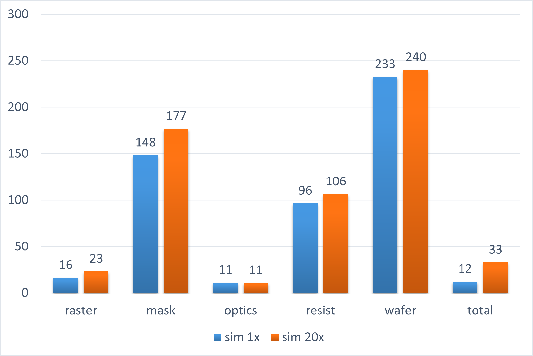
On NVIDIA V100 32-GB GPUs, we demonstrated over 10x speedup in ILT computations as compared to our typical CPU runs. In many key components of the optical and resist modeling, we saw an over 20x speedup.
The encouraging results have led to further developments. We are currently in the process of production scale calibration and testing of key layers using our in-house ILT engine on an NVIDIA A100 80-GB GPU cluster.
Future opportunities with ILT
Advanced chip design increasingly relies on expensive simulations: from circuit performance and timing to thermal dissipation. When it comes to manufacturing, OPC/ILT requires a huge amount of computing power, which is expected to increase as we rapidly progress towards the next node.
Employing HPC with GPUs as well as the entire software stack, consistent with the observation in Huang’s Law, will be the key component to successfully rolling out future generation chips on schedule. More specifically, a unified acceleration architecture for HPC + Rendering (Computer Graphics) + ML/DL will enable better chips to be designed and manufactured, which in turn contributes to improving the speed and efficiency of mask patterning and defect detection applications.
In other words, it’s an iterative process of using GPUs to design faster and better GPUs.
To enable the rapid adoption of ILT masks in HVM, all stakeholders must participate in partnerships and collaborations.
- EDA vendors should make sure that its OPC simulation and correction engine can generate curvilinear mask designs, which conform to standard mask rules that outputs into an acceptable file size and format.
- Vendors for mask data preparation (MDP) should align their systems to process these curvilinear mask data.
- Mask inspection and review tool suppliers should upgrade their systems and algorithms to inspect, model, and detect any potential defects.
There’s no doubt that curvilinear ILT mask designs provide circuit designers with greater freedom and creativity to create circuits with better performance while enabling better process margins with greatly simplified design rules. The benefits of using curvilinear design will have a significant impact on the semiconductor industry and ILT will be the key enabler to the future development of process nodes.