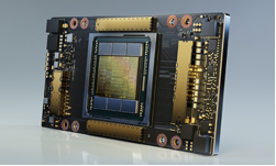
NVIDIA today introduced the first GPU based on the NVIDIA Ampere architecture, the NVIDIA A100, is in full production and shipping to customers worldwide.
The A100 draws on design breakthroughs in the NVIDIA Ampere architecture — offering the company’s largest leap in performance to date within its eight generations of GPUs — to unify AI training and inference and boost performance by up to 20x over its predecessors. A universal workload accelerator, the A100 is also built for data analytics, scientific computing and cloud graphics.
New elastic computing technologies built into A100 make it possible to bring right-sized computing power to every job. A multi-instance GPU capability allows each A100 GPU to be partitioned into as many as seven independent instances for inferencing tasks, while third-generation NVIDIA NVLink interconnect technology allows multiple A100 GPUs to operate as one giant GPU for ever larger training tasks.
The NVIDIA A100 GPU is a technical design breakthrough fueled by five key innovations:
- NVIDIA Ampere architecture — At the heart of A100 is the NVIDIA Ampere GPU architecture, which contains more than 54 billion transistors, making it the world’s largest 7-nanometer processor.
- Third-generation Tensor Cores with TF32 — NVIDIA’s widely adopted Tensor Cores are now more flexible, faster and easier to use. Their expanded capabilities include new TF32 for AI, which allows for up to 20x the AI performance of FP32 precision, without any code changes. In addition, Tensor Cores now support FP64, delivering up to 2.5x more compute than the previous generation for HPC applications.
- Multi-instance GPU — MIG, a new technical feature, enables a single A100 GPU to be partitioned into as many as seven separate GPUs so it can deliver varying degrees of compute for jobs of different sizes, providing optimal utilization and maximizing return on investment.
- Third-generation NVIDIA NVLink — Doubles the high-speed connectivity between GPUs to provide efficient performance scaling in a server.
- Structural sparsity — This new efficiency technique harnesses the inherently sparse nature of AI math to double performance.
Together, these new features make the NVIDIA A100 ideal for diverse, demanding workloads, including AI training and inference as well as scientific simulation, conversational AI, recommender systems, genomics, high-performance data analytics, seismic modeling and financial forecasting.
For more details, read the technical developer blog “NVIDIA Ampere Architecture In-Depth” >>