As the latest member of the NVIDIA Blackwell architecture family, the NVIDIA Blackwell Ultra GPU builds on core innovations to accelerate training and AI reasoning. It fuses silicon innovations with new levels of system-level integration, delivering next-level performance, scalability, and efficiency for AI factories and the large-scale, real-time AI services they power.
With its energy-efficient dual-reticle design, high bandwidth and large-capacity HBM3E memory subsystem, fifth-generation Tensor Cores, and breakthrough NVFP4 precision format, Blackwell Ultra is raising the bar for accelerated computing. This in-depth look explains the architectural advances, why they matter, and how they translate into measurable gains for AI workloads.
Dual-reticle design: one GPU
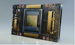
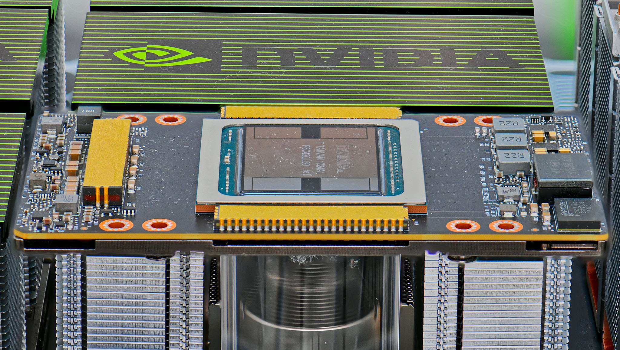
Blackwell Ultra is composed of two reticle-sized dies connected using NVIDIA High-Bandwidth Interface (NV-HBI), a custom, power-efficient die-to-die interconnect technology that provides 10 TB/s of bandwidth. Blackwell Ultra is manufactured using TSMC 4NP and features 208B transistors–2.6x more than the NVIDIA Hopper GPU—all while functioning as a single, NVIDIA CUDA-programmed accelerator. This enables a large increase in performance while also maintaining the familiar CUDA programming model that developers have enjoyed for nearly two decades.
Benefits
- Unified compute domain: 160* Streaming Multiprocessors (SMs) across two dies, providing 640 fifth-generation Tensor Cores with 15 PetaFLOPS dense NVFP4 compute.
- Full coherence: Shared L2 cache with fully coherent memory accesses.
- Maximum silicon utilization: Peak performance per square millimeter.

* Blackwell Ultra GPUs contain up to 160 SMs and 288GB HBM3E Memory. Available SM count and HBM capacity varies by SKU.
Streaming multiprocessors: compute engines for the AI Factory
As shown in Figure 1, the heart of Blackwell Ultra is its 160 Streaming Multiprocessors (SMs) organized into eight Graphics Processing Clusters (GPCs) in the full GPU implementation. Every SM, shown in Figure 2, is a self-contained compute engine housing:
- 128 CUDA Cores for FP32 and INT32 operations, also FP16/BF16 and other precisions.
- 4 fifth-generation Tensor Cores with NVIDIA second-generation Transformer Engine, optimized for FP8, FP6, and NVFP4.
- 256 KB of Tensor Memory (TMEM) for warp-synchronous storage of intermediate results, enabling higher reuse and reduced off-chip memory traffic.
- Special Function Units (SFUs) for transcendental math and special operations used in AI kernels.

NVIDIA Tensor Cores, AI compute powerhouses
When NVIDIA first introduced Tensor Cores in the Volta architecture, they fundamentally changed what GPUs could do for deep learning. Instead of executing scalar or vector operations one element at a time, Tensor Cores operate directly on small matrices—performing matrix multiply-accumulate (MMA) in a single instruction. This was a perfect match for neural networks, where the vast majority of computation comes down to multiplying and summing large grids of numbers.
Over successive generations, Tensor Cores have expanded in capability, precision formats, and parallelism:
- NVIDIA Volta: 8-thread MMA units, FP16 with FP32 accumulation for training.
- NVIDIA Ampere: Full warp-wide MMA, BF16, and TensorFloat-32 formats.
- NVIDIA Hopper: Warp-group MMA across 128 threads, Transformer Engine with FP8 support.
Blackwell and Blackwell Ultra take this to the next level with their fifth-generation Tensor Cores and second-generation Transformer Engine, delivering higher throughput and lower latency for both dense and sparse AI workloads. Each Streaming Multiprocessor (SM) contains four Tensor Cores across the 160 SMs in Blackwell Ultra, adding up to 640 Tensor Cores upgraded to handle the newest precision format, NVFP4.
These enhancements aren’t just about raw FLOPS. The new Tensor Cores are tightly integrated with 256 KB of Tensor Memory (TMEM) per SM, optimized to keep data close to the compute units. They also support dual-thread-block MMA, where paired SMs cooperate on a single MMA operation, sharing operands and reducing redundant memory traffic.
The result is higher sustained throughput, better memory efficiency, and faster large-batch pre-training, reinforcement learning for post-training, and low-batch, high-interactivity inference.
Ultra-charged NVFP4 performance
The introduction of NVIDIA NVFP4, the new 4‑bit floating‑point format in the Blackwell GPU architecture, combines two-level scaling—an FP8 (E4M3) micro-block scale applied to 16‑value blocks plus a tensor-level FP32 scale—enabling hardware‑accelerated quantization with markedly lower error rates than standard FP4. This Tensor Core capability delivers nearly FP8‑equivalent accuracy (with often less than ~1% difference), while reducing memory footprint by ~1.8x compared to FP8 and up to ~3.5x vs. FP16. NVFP4 strikes an optimal balance of accuracy, efficiency, and performance for low‑precision AI inference.
The Blackwell Ultra dense NVFP4 compute capability provides a substantial performance uplift over the original Blackwell GPU. While the base architecture delivers 10 petaFLOPS of NVFP4 performance, Ultra pushes that to 15 petaFLOPS—a 1.5x increase compared to Blackwell GPU and 7.5x increase from NVIDIA Hopper H100 and H200 GPUs, as shown in Figure 3. This boost directly benefits large-scale inference, enabling more concurrent model instances, faster response times, and lower costs per token generated.

Accelerated softmax in the attention layer
Modern AI workloads rely heavily on attention processing with long input contexts and long output sequences for “thinking”. Transformer attention layers, in turn, stress exponentials, divisions, and other transcendental operations executed by the SM’s SFUs.
In Blackwell Ultra, SFU throughput has been doubled for key instructions used in attention, delivering up to 2x faster attention-layer compute compared to Blackwell GPUs. This improvement accelerates both short and long-sequence attention, but is especially impactful for reasoning models with large context windows—where the softmax stage can become a latency bottleneck.
By accelerating the attention mechanism within transformer models, Blackwell Ultra enables:
- Faster AI reasoning with lower time-to-first-token in interactive applications.
- Lower compute costs by reducing total processing cycles per query.
- Higher system efficiency—more attention sequences processed per watt.
As depicted in Figure 4, the performance gains from the accelerated attention-layer instructions in Blackwell Ultra compound with NVFP4 precision, resulting in a step-function improvement for LLM and multimodal inference.

Memory: high capacity and bandwidth for multi-trillion-parameter models
Blackwell Ultra doesn’t just scale compute—it scales memory capacity to meet the demands of the largest AI models. With 288 GB of HBM3e per GPU, it offers 3.6x more on-package memory than H100 and 50% more than Blackwell, as shown in Figure 5. This capacity is critical for hosting trillion-parameter models, extending context length without KV-cache offloading, and enabling high-concurrency inference in AI factories.
High bandwidth memory features
- Max capacity: 288 GB, 3.6x increase over H100
- HBM configuration: Eight 12-Hi stacks, 16 × 512-bit controllers (8,192-bit total width)
- Bandwidth: 8 TB/s per GPU, 2.4x improvement over H100 (3.35 TB/s)

This massive memory footprint enables:
- Complete model residence: 300B+ parameter models without memory offloading.
- Extended context lengths: Larger KV cache capacity for transformer models.
- Improved compute efficiency: Higher compute-to-memory ratios for diverse workloads.
Interconnect: built for scale
Blackwell and Blackwell Ultra support fifth-generation NVIDIA NVLink for GPU-to-GPU communication over NVLink Switch, NVLink-C2C for coherent interconnect to an NVIDIA Grace CPU, and x16 PCI-Express Gen 6 interface for connection to host CPUs.
NVLink 5 Specifications
- Per-GPU Bandwidth: 1.8 TB/s bidirectional (18 links x 100 GB/s)
- Performance Scaling: 2x improvement over NVLink 4 (Hopper GPU)
- Maximum Topology: 576 GPUs in non-blocking compute fabric
- Rack-Scale Integration: 72-GPU NVL72 configurations with 130 TB/s aggregate bandwidth
Host connectivity:
- PCIe Interface: Gen6 × 16 lanes (256 GB/s bidirectional)
- NVLink-C2C: Grace CPU-GPU communication with memory coherency (900 GB/s)
Table 1 provides a comparison of the interconnects across generations.
| Interconnect | Hopper GPU | Blackwell GPU | Blackwell Ultra GPU |
|---|---|---|---|
| NVLink (GPU-GPU) | 900 | 1,800 | 1,800 |
| NVLink-C2C (CPU-GPU) | 900 | 900 | 900 |
| PCIe Interface | 128 (Gen 5) | 256 (Gen 6) | 256 (Gen 6) |
Advancing performance-efficiency
Blackwell Ultra delivers a decisive leap over Blackwell by adding 50% more NVFP4 compute and 50% more HBM capacity per chip, enabling larger models and faster throughput without compromising efficiency. Accelerated softmax execution further boosts real-world inference speeds, driving up tokens per second per user (TPS/user) while improving data center tokens per second per megawatt (TPS/MW). Every architectural enhancement was purpose-built to push both user experience and operational efficiency to the next level.
As shown in Figure 6, plotting these two metrics for the NVIDIA Hopper HGX H100 NVL8 system, NVIDIA Blackwell HGX B200 NVL8 system, NVIDIA Blackwell GB200 NVL72 system, and NVIDIA Blackwell Ultra GB300 NVL72 system reveals a generational leap. The curve starts with Hopper NVL8 at FP8 precision and ends with Blackwell Ultra NVL72 at NVFP4 precision—showing how each architectural advance pushes the Pareto frontier up and to the right.

These architectural innovations improve the economics of AI inference and redefine what’s possible in AI factory design—delivering more model instances, faster responses, and higher output per megawatt than any previous NVIDIA platform.
To see firsthand how innovations in hardware and deployment configurations impact data center efficiency and user experience, check out our interactive Pareto Frontier explainer.
Enterprise-grade features
Blackwell Ultra isn’t just about raw performance—it’s designed with enterprise-grade features that simplify operations, strengthen security, and deliver reliable performance at scale.
Advanced scheduling and management
- Enhanced GigaThread Engine: Next-generation work scheduler providing improved context switching performance and optimized workload distribution across all 160 SMs.
- Multi-Instance GPU (MIG): Blackwell Ultra GPUs can be partitioned into different-sized MIG instances. For example, an administrator can create two instances with 140 GB of memory each, four instances with 70 GB each, or seven instances with 34 GB each, enabling secure multi-tenancy with predictable performance isolation.
Security and reliability
- Confidential computing and secure AI: Secure and performant protection for sensitive AI models and data, extending hardware-based Trusted Execution Environment (TEE) to GPUs with industry-first TEE-I/O capabilities in the Blackwell architecture and inline NVLink protection for near-identical throughput when compared to unencrypted modes.
- Advanced NVIDIA Reliability, Availability, and Serviceability (RAS) engine: AI-powered reliability system monitoring thousands of parameters to predict failures, optimize maintenance schedules, and maximize system uptime in large-scale deployments.
AI video and data processing enhancements
Blackwell Ultra also integrates specialized engines for modern AI workloads requiring multimodal data processing:
- Video and JPEG decoding: The NVIDIA Video Decoder (NVDEC) and NVIDIA JPEG Decoder (NVJPEG) engines are specialized fixed-function hardware units for high-throughput image and video processing.
- NVDEC supports modern codecs like AV1, HEVC, and H.264, enabling batch or real-time video decoding directly on the GPU without using CUDA Cores.
- NVJPEG accelerates JPEG decompression in hardware, making large-scale image pipelines dramatically faster.
- Both engines are leveraged by NVIDIA DALI (Data Loading Library), which integrates them into AI training and inference workflows for tasks like image augmentation, dataset preprocessing, and multimodal model input preparation.
- Decompression engine: Hardware-accelerated data decompression at 800 GB/s throughput, reducing CPU overhead and accelerating compressed dataset loading for analytics workloads. NVIDIA nvCOMP enables portable programming of the decompression engine.
NVIDIA GPU chip summary comparison
To put Blackwell Ultra’s advances in perspective, Table 2 compares key chip specifications across Hopper, Blackwell, and Blackwell Ultra. It highlights the generational leap in transistor count, memory capacity, interconnect bandwidth, and precision compute throughput—as well as the architectural enhancements like attention acceleration and NVFP4. This side-by-side view shows how Blackwell Ultra scales up performance and extends capabilities critical for AI factory deployments at both node and rack scale.
| Feature | Hopper | Blackwell | Blackwell Ultra |
|---|---|---|---|
| Manufacturing process | TSMC 4N | TSMC 4NP | TSMC 4NP |
| Transistors | 80B | 208B | 208B |
| Dies per GPU | 1 | 2 | 2 |
| NVFP4 dense | sparse performance | – | 10 | 20 PetaFLOPS | 15 | 20 PetaFLOPS |
| FP8 dense | sparse performance | 2 | 4 PetaFLOPS | 5 | 10 PetaFLOPS | 5 | 10 PetaFLOPS |
| Attention acceleration (SFU EX2) | 4.5 TeraExponentials/s | 5 TeraExponentials/s | 10.7 TeraExponentials/s |
| Max HBM capacity | 80 GB HBM (H100) 141 GB HBM3E (H200) | 192 GB HBM3E | 288 GB HBM3E |
| Max HBM bandwidth | 3.35 TB/s (H100) 4.8 TB/s (H200) | 8 TB/s | 8 TB/s |
| NVLink bandwidth | 900 GB/s | 1,800 GB/s | 1,800 GB/s |
| Max power (TGP) | Up to 700W | Up to 1,200W | Up to 1,400W |
From chip to AI factory
Blackwell Ultra GPUs form the backbone of NVIDIA’s next-generation AI infrastructure—delivering transformative performance from desktop superchips to full AI factory racks.
NVIDIA Grace Blackwell Ultra Superchip
This superchip couples one Grace CPU with two Blackwell Ultra GPUs through NVLink‑C2C, offering up to 30 PFLOPS dense, and 40 PFLOPS sparse, NVFP4 AI compute, and boasts 1 TB of unified memory combining HBM3E and LPDDR5X for unprecedented on-node capacity. ConnectX-8 SuperNICs provide 800 Gb/s high-speed network connectivity (See Figure 7). The NVIDIA Grace Blackwell Ultra Superchip is the foundational computing component of the GB300 NVL 72 rack-scale system.

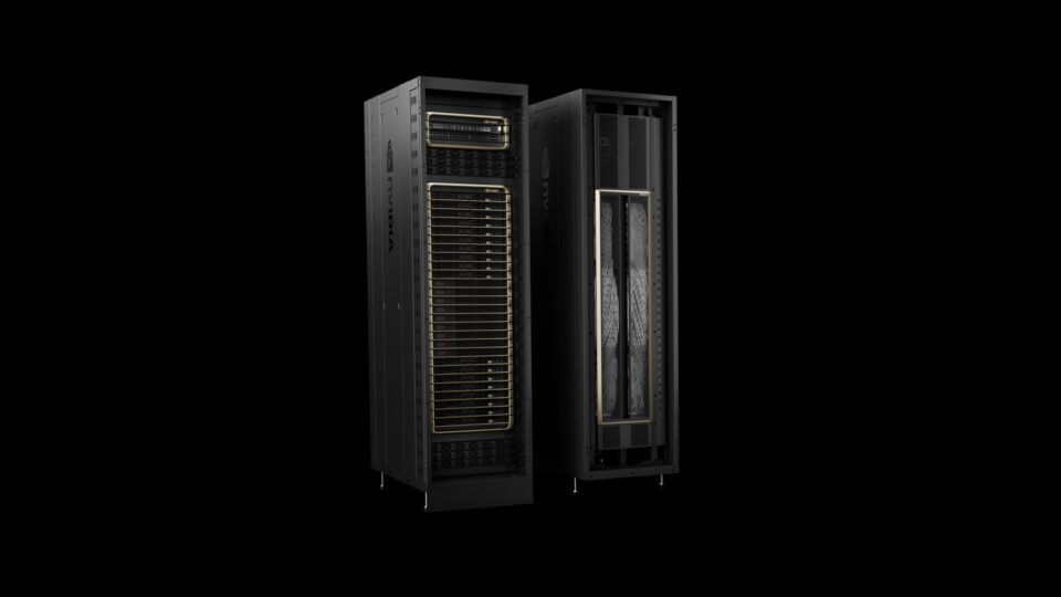
- NVIDIA GB300 NVL72 rack-scale system: This liquid-cooled rack integrates 36 Grace Blackwell Superchips, interconnected through NVLink 5 and NVLink Switching, enabling it to achieve 1.1 exaFLOPS dense FP4 compute. The GB300 NVL72 also enables a 50x higher AI factory output, combining 10x better latency (TPS per user) and 5x higher throughput per megawatt relative to Hopper platforms. GB300 systems also redefine rack power management. They rely on multiple power-shelf configurations to handle synchronous GPU load ramps. NVIDIA power smoothing innovations—including energy storage and burn mechanisms—help stabilize power draw across training workloads.
- NVIDIA HGX and DGX B300 systems: Standardized 8 GPU Blackwell Ultra configurations. NVIDIA HGX B300 and NVIDIA DGX B300 Systems continue to support flexible deployment models for AI infrastructure while maintaining full CUDA and NVLink compatibility.
Complete CUDA compatibility
Blackwell Ultra maintains full backward compatibility with the entire CUDA ecosystem while introducing optimizations for next-generation AI frameworks:
- Framework integration: Native support in SGLang, TensorRT-LLM, and vLLM with optimized kernels for NVFP4 precision and dual-die architecture.
- NVIDIA Dynamo: A distributed inference and scheduling framework that intelligently orchestrates workloads across thousands of GPUs, delivering up to 30x higher throughput for large-scale deployments.
- NVIDIA Enterprise AI: End-to-end, cloud-native AI software platform delivering optimized frameworks, SDKs, microservices, and enterprise-grade tools for developing, deploying, and managing AI workloads at scale.
- NVIDIA development tools and CUDA libraries:
- CUTLASS for custom kernel development
- Nsight Systems and Nsight Compute for profiling and tuning
- Model Optimizer for precision-aware graph optimization
- cuDNN for deep learning primitives
- NCCL for multi-GPU communication
- CUDA Graphs for reducing launch overhead
The bottom line
NVIDIA Blackwell Ultra establishes the foundation for AI factories to train and deploy intelligence at unprecedented scale and efficiency. With breakthrough innovations in dual-die integration, NVFP4 acceleration, massive memory capacity, and advanced interconnect technology, Blackwell Ultra enables AI applications that were previously computationally impossible.
As the industry transitions from proof-of-concept AI to production AI factories, Blackwell Ultra provides the computational foundation to turn AI ambitions into reality with unmatched performance, efficiency, and scale.
Learn more
Dive deeper into the innovations powering the trillion-token era. Download the Blackwell Architecture Technical Brief to explore the full silicon-to-system story.
Acknowledgments
We’d like to thank Manas Mandal, Ronny Krashinsky, Vishal Mehta, Greg Palmer, Michael Andersch, Eduardo Alvarez, Ashraf Eassa, Joe DeLaere, and many other NVIDIA GPU architects, engineers, and product leaders who contributed to this post.
This post was updated on 9/24/25 to correct Figure 1 and the HBM configuration section to show the proper 12 HBM stacks instead of 8.