In the heart of every modern electronic device lies a silicon chip, built through a manufacturing process so precise that even a microscopic defect can determine success or failure. As semiconductor devices grow more complex, reliably detecting and classifying defects has become a critical bottleneck.
Historically, chipmakers have relied on convolutional neural networks (CNNs) to automate defect classification (ADC). But as manufacturing scales and diversifies, CNN-based approaches are hitting their limits, requiring large labeled datasets, frequent retraining, and still struggling to generalize across new defect types.
In this post, we show how generative AI-powered ADC can overcome these challenges.
The workflows below leverage NVIDIA Metropolis vision language models (VLMs), vision foundation models (VFMs), and the NVIDIA TAO fine-tuning toolkit to modernize defect classification. We outline the limitations of traditional CNN-based systems, detail how VLMs and VFMs address them, and highlight specific approaches and manufacturing challenges they help solve.
The limits of CNNs in semiconductor defect classification
CNNs have long been the backbone of defect detection in semiconductor fabs, supporting optical and e-beam inspection, lithographic analysis, and more. They excel at extracting visual features from large datasets, but manufacturers face persistent challenges related to data requirements, semantic understanding, and retraining.
High data requirements
Achieving high accuracy often requires thousands of labeled images per defect class. Rare or emerging defects frequently lack sufficient examples for effective training.
Limited semantic understanding
While CNNs capture visual features, they cannot interpret context, perform root-cause analysis, or integrate multimodal data. They also struggle to differentiate visually similar yet operationally distinct defect patterns, such as center vs. local defects.
Frequent retraining
Real-world manufacturing is dynamic. Process variations, new tools, and evolving product lines require models to be retrained frequently to recognize new defect types and imaging conditions.
These limitations force fabs to rely on manual inspection, which is costly, inconsistent, and unable to scale with today’s manufacturing throughput.
Modernizing ADC with VLMs and VFMs
To address these challenges, NVIDIA applies VLMs, VFMs, and self-supervised learning across multiple stages of semiconductor manufacturing. Figure 1 illustrates how these models are deployed across front-end-of-line (FEOL) and back-end packaging processes.
In this post, we demonstrate how VLMs classify wafer map images and how VFMs classify die-level images, including optical, e-beam, and back-end optical microscopy (OM) inspection data. With further training, VLMs also show strong potential for die-level inspection.

Wafer-level intelligence with VLMs
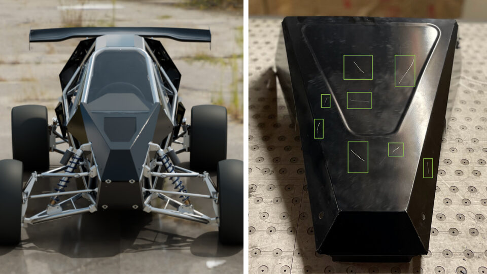
Wafer maps provide a spatial view of defect distributions across an entire wafer. VLMs combine advanced image understanding with natural language reasoning. After fine-tuning, NVIDIA reasoning VLMs, such as Cosmos Reason, can interpret wafer map images to identify macro defects, generate natural language explanations, perform interactive Q&A, and compare test images against “golden” references for preliminary root-cause analysis.

Using this approach offers several advantages:
- Few-shot learning: VLMs can be fine-tuned with only a small number of labeled examples, enabling rapid adaptation to new defect patterns, process changes, or product variations.
- Explainability: As shown in Figure 2, Cosmos Reason produces interpretable results that engineers can interact with using natural language. For example, asking “What is the primary defect pattern in this wafer map?” might return “Center ring defect detected, likely due to chemical contamination.” This semantic reasoning ability goes beyond CNNs, helping engineers quickly identify potential root causes, accelerate corrective actions, and reduce the volume of manual reviews.
- Automated data labeling: VLMs can generate high-quality labels for downstream ADC tasks, reducing the time and cost of model development. In practice, this approach can cut model build times by up to 2x compared to manual labeling workflows.
- Time series and lot level analysis: VLMs have the ability to process both still images and video sequences, enabling them to proactively monitor process anomalies over time and mitigate errors before they lead to critical failures. In one study, VLMs achieved high accuracy across both OK and NG cases, outperforming traditional CNN-based methods.

Getting started with Cosmos Reason
Here’s a sample workflow to fine-tune Cosmos Reason 1—from data preparation to supervised fine-tuning and evaluation on a prepared dataset of wafer map defects.
- Go to the Cosmos Cookbook Wafer Map Anomaly Classification
- Create a sample training dataset: Download the open WM-811k Wafermap dataset produced by Mir Lab which is available for public use. Generate a sample dataset and respective annotations with the provided scripts in the cookbook.
- Post-train with supervised fine-tuning (SFT): Follow the installation instructions provided in the cosmos-reason1 GitHub repository and install the cosmos-rl package to enable fine-tuning with the curated training data set.
- Deploy
Result: Fine-tuning Cosmos Reason on wafer map defect classification data boosts accuracy from zero-shot levels to over 96% on defect classification tasks.
Die-level precision with VFMs and self-supervised learning
The semiconductor industry continues to push the boundaries of physics as device features shrink to microscopic scales. At this level, manufacturing complexity rises dramatically. Even the slightest anomaly—a stray particle, pattern deviation, or material defect—can render a chip unusable, directly affecting yield and profitability. In this high-stakes environment, the biggest bottleneck is the ability to rapidly and accurately detect and classify defects. CNNs have supported this workflow for years, but they struggle to keep pace with the growing complexity and data demands of modern fabs.
A core challenge in training AI models for manufacturing is the dependence on large, meticulously labeled datasets. Dynamic processes, evolving product lines, and the continual emergence of new defect types make it impractical to maintain a perfectly labeled dataset. Compounding the issue, datasets are often highly imbalanced—normal samples vastly outnumber defective ones.
Using a leading VFM such as NV-DINOv2 provides advantages, including:
- Self-supervised learning (SSL): NV-DINOv2 is trained on millions of unlabeled images, enabling it to generalize new defect types and process conditions with minimal retraining when labeled data is scarce.
- Robust feature extraction: The model captures both fine-grained visual details and high-level semantic information, improving classification accuracy across diverse manufacturing scenarios.
- Operational efficiency: By reducing dependence on labeling and frequent retraining, NV-DINOv2 streamlines the deployment and maintenance of defect-inspection systems in fast-moving fab environments.
However, general foundation models like NV-DINOv2 lack the specific details required for industrial tasks such as e-beam and optical microscopy images. To achieve maximum accuracy, the model must be specialized through domain adaptation.
This is a multi-stage workflow:
- General VFM: Begin with the powerful, pre-trained NV-DINOv2 model that has broad visual understanding learned from large, diverse datasets.
- Domain adaptation: Fine-tune the model using a large, unlabeled, domain-specific dataset, such as millions of images from semiconductor fabs, to align it with industrial imaging characteristics.
- Downstream task fine-tuning: Apply a small set of labeled images to fine-tune the model for a specific classification task, a step known as linear probing.

The effectiveness of this process depends heavily on the size and quality of the unlabeled domain dataset. These datasets can range from less than a million images to hundreds of millions, but quantity alone is not enough. A meticulous data-cleaning pipeline is essential to remove redundant, blurry, or irrelevant images before training begins.
This domain-adaptation approach delivers significant performance gains. In one study by a leading semiconductor manufacturer, the NVIDIA TAO Toolkit was used to apply self-supervised learning (SSL) to NV-DINOv2 using unlabeled images collected across multiple layers of the chip-production process. Incorporating SSL consistently improved performance, boosting accuracy by up to 8.9% compared to a model trained without SSL which led to productivity gains of up to 9.9%.
Getting started with NV-DINOv2 and SSL
The following is an end-to-end workflow to fine-tune NV-DINOv2 using SSL, from data preparation and domain adaptation to downstream task fine-tuning and deployment. In this example, we use the NVIDIA TAO Toolkit to perform SSL on unlabeled PCB images for defect classification.
The NV-DINOv2 workflow follows a progressive, three-phase approach that maximizes the value of large unlabeled datasets while reducing the need for manual annotation to only a few hundred labeled samples.
1. Set up your environment: Download the NVIDIA TAO Toolkit 6.0 container from NVIDIA NGC which has all dependencies pre-installed:
# Pull the TAO Toolkit 6.0 container from NGC
docker pull nvcr.io/nvidia/tao/tao-toolkit:6.0.0-pyt

# Run the container with GPU support
docker run --gpus all -it -v /path/to/data:/data \
	nvcr.io/nvidia/tao/tao-toolkit:6.0.0-pyt /bin/bash
2. Prepare your dataset: NV-DINOv2 accepts RGB images in standard formats (JPG, PNG, BMP, TIFF, WebP) stored in a single directory. For SSL domain adaptation, you only need unlabeled images; no annotations are required.
In our PCB inspection example, we used:
- ~400 labeled test samples for evaluation
- ~One million unlabeled PCB images for domain adaptation
- ~600 labeled training samples for downstream fine-tuning
Organize your data as followed:
/data/
├── unlabeled_images/      	# For SSL domain adaptation
├── train_images/          	# For downstream fine-tuning
│   ├── OK/
│   ├── missing/
│   ├── shift/
│   ├── upside_down/
│   ├── poor_soldering/
│   └── foreign_object/
└── test_images/           	# For evaluation
Data cleaning best practice: Before training, perform a meticulous data cleaning process to remove redundant, blurry, or irrelevant images. The effectiveness of domain adaptation depends heavily on the quality of your unlabeled dataset.
3. Configure the training specification: Create a YAML specification file that defines your model architecture, dataset paths, and training parameters:
model:
  backbone:
    teacher_type: "vit_l"
    student_type: "vit_l"
    patch_size: 14
    img_size: 518
    drop_path_rate: 0.4
  head:
    num_layers: 3
    hidden_dim: 2048
    bottleneck_dim: 384


dataset:
  train_dataset:
    images_dir: /data/unlabeled_images
  test_dataset:
    images_dir: /data/test_images
  batch_size: 16
  workers: 10
  transform:
    n_global_crops: 2
    global_crops_scale: [0.32, 1.0]
    global_crops_size: 224
    n_local_crops: 8
    local_crops_scale: [0.05, 0.32]
    local_crops_size: 98


train:
  num_gpus: 8
  num_epochs: 100
  checkpoint_interval: 10
  precision: "16-mixed"
  optim:
    optim: "adamw"
  clip_grad_norm: 3.0
4. Run SSL training for domain adaptation: Execute the training using TAO Launcher to adapt the general NV-DINOv2 model to your domain-specific images:
tao model nvdinov2 train \
	-e /path/to/experiment_spec.yaml \
	results_dir=/output/ssl_training \
	train.num_gpus=8 \
	train.num_epochs=100
5. Perform downstream task fine-tuning: After SSL domain adaptation, fine-tune the model for your specific classification task using a small labeled dataset. This step, known as linear probing, requires only a few hundred labeled samples:
tao model nvdinov2 train \
	-e /path/to/finetune_spec.yaml \
	train.pretrained_model_path=/output/ssl_training/model.pth \
	dataset.train_dataset.images_dir=/data/train_images \
	train.num_epochs=50
6. Run inference: Evaluate your domain-adapted model on test images:
tao model nvdinov2 inference \
	-e /path/to/experiment_spec.yaml \
	inference.checkpoint=/output/ssl_training/model.pth \
	inference.gpu_ids=[0] \
	inference.batch_size=32
7. Export to ONNX for deployment: Export your trained model to ONNX format for production deployment:
tao model nvdinov2 export \
	-e /path/to/experiment_spec.yaml \
	export.checkpoint=/output/ssl_training/model.pth \
	export.onnx_file=/output/nvdinov2_domain_adapted.onnx \
	export.opset_version=12 \
	export.batch_size=-1
The exported ONNX model can be deployed using NVIDIA TensorRT for optimized inference or integrated into an NVIDIA DeepStream pipeline for real-time visual inspection.
Results: Using NVIDIA TAO to fine-tune NV-DINOV2 with SSL can also be used for inspecting PCBs. By using a dataset of approximately one million unlabeled images with SSL for industrial domain adaption and 600 training and 400 testing samples for downstream task fine-tuning, accuracy for defect detection jumped from 93.84% with the general model to 98.51%. By eliminating the need for labeling and frequent retraining, NV-DINOv2 streamlines the deployment of defect inspection solutions in fast-moving fab environments.
Paving the way to a smart fab
These applications of vision models deliver immediate accuracy gains and lay the foundation for agentic AI systems within the fab. By combining accelerated computing with generative AI, NVIDIA and leading foundries are introducing new ADC workflows that have the potential to redefine yield improvement and process control in advanced manufacturing.
By streamlining defect analysis across the semiconductor production flow, generative AI significantly reduces model deployment time. Its few-shot learning capabilities simplify ongoing model maintenance, improve robustness, and make it easy to fine-tune models for different fab environments.
With fabs generating millions of high-resolution images daily from a wide range of inspection tools, automated ADC systems are expected to further improve classification accuracy, reduce human workload, and elevate overall productivity.
Beyond defect inspection, semiconductor manufacturers are beginning to adopt video analytics AI agents built using the NVIDIA Blueprint for Video Search and Summarization (VSS). These agents help monitor plant operations, enhance worker safety, and improve compliance with PPE and safety protocols across manufacturing sites.
Next steps
To learn more, try NV-DINOv2 and state-of-the-art NVIDIA VLMs like Cosmos Reason. For technical questions, please visit the forum.
Watch the SEMICON West keynote from Tim Costa, the General Manager of Industrial and Computational Engineering at NVIDIA, and attend sessions at the show, which runs through December 19
Stay up to date by subscribing to our newsletter and following NVIDIA AI on LinkedIn, Instagram, X and Facebook. Explore YouTube channel, and join the NVIDIA Developer vision AI forum.