At the 2016 GPU Technology Conference in San Jose, NVIDIA CEO Jen-Hsun Huang announced the new NVIDIA Tesla P100, the most advanced accelerator ever built. Based on the new NVIDIA Pascal GP100 GPU and powered by ground-breaking technologies, Tesla P100 delivers the highest absolute performance for HPC, technical computing, deep learning, and many computationally intensive datacenter workloads.
Today at ISC 2016 in Frankfurt, NVIDIA expanded the Tesla P100 product family with the new Tesla P100 for PCIe-based servers.
In this post, I provide an overview of the Pascal architecture and its benefits to you as a developer.
At GTC, Lars Nyland and I gave a talk about details of the Tesla P100 and the Pascal GP100 architecture. The slides and recording from this talk are now available (GTC on-demand site registration required). To learn more, read the Tesla P100 whitepaper.
Tesla P100: Extreme Performance and Features for GPU Computing
The GP100 GPU used in Tesla P100 incorporates multiple revolutionary new features and unprecedented performance. Key features of Tesla P100 include:
- Extreme performance—powering HPC, deep learning, and many more GPU Computing areas;
- NVLink™ —NVIDIA’s new high speed, high bandwidth interconnect for maximum application scalability;
- HBM2—Fastest, high capacity, extremely efficient stacked GPU memory architecture;
- Unified Memory and Compute Preemption—significantly improved programming model;
- 16nm FinFET—enables more features, higher performance, and improved power efficiency.
Tesla P100 Available for NVLink and PCIe Servers
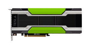
Tesla P100 accelerators will be available in two forms: A traditional GPU accelerator board for PCIe-based servers, and an SXM2 module for NVLink-optimized servers. P100 for PCIe-based servers allows HPC data centers to deploy the most advanced GPUs within PCIe-based nodes to support a mix of CPU and GPU workloads. P100 for NVLink-optimized servers provides the best performance and strong scaling for hyperscale and HPC data centers running applications that scale to multiple GPUs, such as deep learning. The table below provides the complete specifications of both Tesla P100 accelerators.
The Pascal GP100 Architecture: Faster in Every Way
With every new GPU architecture, NVIDIA introduces major improvements to performance and power efficiency. The heart of the computation in Tesla GPUs is the streaming multiprocessor (SM). The SM creates, manages, schedules, and executes instructions from many threads in parallel.
Like previous Tesla GPUs, GP100 is composed of an array of graphics processing clusters (GPCs), SMs, and memory controllers. GP100 achieves its colossal throughput by providing six GPCs, up to 60 SMs, and eight 512-bit memory controllers (4096 bits total).
The Pascal architecture’s computational prowess is more than just brute force: it increases performance not only by adding more SMs than previous GPUs, but by making each SM more efficient. Each SM has 64 CUDA cores and four texture units, for a total of 3840 CUDA cores and 240 texture units.
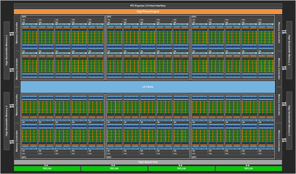
Delivering higher performance and improving energy efficiency are two key goals for new GPU architectures. A number of changes to the SM in the Maxwell architecture improved its efficiency compared to Kepler. Pascal builds on this and incorporates additional improvements that increase performance per watt even further over Maxwell.
While TSMC’s 16nm Fin-FET manufacturing process plays an important role, many GPU architectural modifications were also implemented to further reduce power consumption while maintaining high performance.
The following table provides a high-level comparison of Tesla P100 specifications compared to previous-generation Tesla GPU accelerators.
| Tesla Products | Tesla K40 | Tesla M40 | Tesla P100 (NVLink) | Tesla P100 (PCIe) |
| GPU / Form Factor | Kepler GK110 / PCIe | Maxwell GM200 / PCIe | Pascal GP100 / SXM2 | Pascal GP100 / PCIe |
| SMs | 15 | 24 | 56 | 56 |
| TPCs | 15 | 24 | 28 | 28 |
| FP32 CUDA Cores / SM | 192 | 128 | 64 | 64 |
| FP32 CUDA Cores / GPU | 2880 | 3072 | 3584 | 3584 |
| FP64 CUDA Cores / SM | 64 | 4 | 32 | 32 |
| FP64 CUDA Cores / GPU | 960 | 96 | 1792 | 1792 |
| Base Clock | 745 MHz | 948 MHz | 1328 MHz | 1126 MHz |
| GPU Boost Clock | 810/875 MHz | 1114 MHz | 1480 MHz | 1303 MHz |
| FP32 GFLOPs[1] | 5040 | 6844 | 10608 | 9340 |
| FP64 GFLOPs[1] | 1680 | 213 | 5304 | 4670 |
| Texture Units | 240 | 192 | 224 | 224 |
| Memory Interface | 384-bit GDDR5 | 384-bit GDDR5 | 4096-bit HBM2 | 3072-bit HBM2 (12GB) 4096-bit HBM2 (16GB) |
| Memory Bandwidth | 288 GB/s | 288 GB/s | 732 GB/s | 549 GB/s (12GB) 732 GB/s (16GB) |
| Memory Size | Up to 12 GB | Up to 24 GB | 16 GB | 12 GB or 16 GB |
| L2 Cache Size | 1536 KB | 3072 KB | 4096 KB | 4096 KB |
| Register File Size / SM | 256 KB | 256 KB | 256 KB | 256 KB |
| Register File Size / GPU | 3840 KB | 6144 KB | 14336 KB | 14336 KB |
| TDP | 235 Watts | 250 Watts | 300 Watts | 250 Watts |
| Transistors | 7.1 billion | 8 billion | 15.3 billion | 15.3 billion |
| GPU Die Size | 551 mm² | 601 mm² | 610 mm² | 610 mm² |
| Manufacturing Process | 28-nm | 28-nm | 16-nm | 16-nm |
[1] The GFLOPS in this chart are based on GPU Boost Clocks.
Pascal streaming multiprocessor
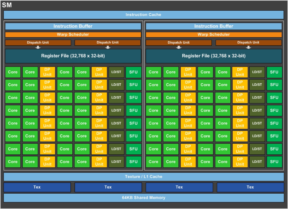
GP100’s SM incorporates 64 single-precision (FP32) CUDA Cores. In contrast, the Maxwell and Kepler SMs had 128 and 192 FP32 CUDA Cores, respectively. The GP100 SM is partitioned into two processing blocks, each having 32 single-precision CUDA Cores, an instruction buffer, a warp scheduler, and two dispatch units.
While a GP100 SM has half the total number of CUDA Cores of a Maxwell SM, it maintains the same register file size and supports similar occupancy of warps and thread blocks.
GP100’s SM has the same number of registers as Maxwell GM200 and Kepler GK110 SMs, but the entire GP100 GPU has far more SMs, and thus many more registers overall. This means threads across the GPU have access to more registers, and GP100 supports more threads, warps, and thread blocks in flight compared to prior GPU generations.
Overall shared memory across the GP100 GPU is also increased due to the increased SM count, and aggregate shared memory bandwidth is effectively more than doubled. A higher ratio of shared memory, registers, and warps per SM in GP100 allows the SM to execute code more efficiently.
There are more warps for the instruction scheduler to choose from, more loads to initiate, and more per-thread bandwidth to shared memory (per thread).
Compared to Kepler, Pascal’s SM features a simpler datapath organization that requires less die area and less power to manage data transfers within the SM. Pascal also provides superior scheduling and overlapped load/store instructions to increase floating point utilization.
The new SM scheduler architecture in GP100 improves upon the advances of the Maxwell scheduler and is even more intelligent, providing increased performance and reduced power consumption. Each warp scheduler (one per processing block) is capable of dispatching two warp instructions per clock.
High-Performance Double Precision
Because of the importance of high-precision computation for technical computing and HPC codes, a key design goal for Tesla P100 is high double-precision performance. Each GP100 SM has 32 FP64 units, providing a 2:1 ratio of single- to double-precision throughput. Compared to the 3:1 ratio in Kepler GK110 GPUs, this allows Tesla P100 to process FP64 workloads more efficiently.
Like previous GPU architectures, GP100 supports full IEEE 754‐2008 compliant single- and double‐precision arithmetic, including support for the fused multiply‐add (FMA) operation and full speed support for denormalized values.
FP16 Arithmetic Support for Faster Deep Learning
The rapidly growing field of deep learning is one of the fastest growing fields of computing. Deep learning has proven to provide a high-level of accuracy and adaptability in applications spanning automatic image captioning, autonomous driving object recognition, natural language understanding and translation, and even computer-generated art. For an in-depth introduction to deep learning, check out the Deep Learning in a Nutshell series here on Parallel Forall.
Unlike other technical computing applications that require high-precision floating-point computation, deep neural network architectures have a natural resilience to errors due to the backpropagation algorithm used in their training. Storing FP16 data compared to higher precision FP32 or FP64 reduces memory usage of the neural network, allowing training and deployment of larger networks. Using FP16 computation improves performance up to 2x compared to FP32 arithmetic, and similarly FP16 data transfers take less time than FP32 or FP64 transfers.
The GP100 SM ISA provides new arithmetic operations that can perform two FP16 operations at once on a single-precision CUDA Core, and 32-bit GP100 registers can store two FP16 values.
Improved Atomics
Atomic memory operations are important in parallel programming, allowing concurrent threads to correctly perform read-modify-write operations on shared data. Kepler significantly increased the throughput of atomic operations to global memory compared to the earlier Fermi architecture; however, both Fermi and Kepler implemented shared memory atomics using an expensive lock/update/unlock pattern.
Maxwell improved this by implementing native hardware support for shared memory atomic operations for 32-bit integers, and native shared memory 32-bit and 64-bit compare-and-swap (CAS), which can be used to implement other atomic functions with reduced overhead (compared to the Fermi and Kepler methods which were implemented in software).
GP100 further improves atomics by providing an FP64 atomic add instruction for values in global memory. The `atomicAdd()“ function in CUDA now applies to 32 and 64-bit integer and floating-point data. Previously, FP64 atomic addition had to be implemented using a compare-and-swap loop, which is generally slower than a native instruction.
Compute Capability 6.0
GP100 supports the new Compute Capability 6.0. The following table compares parameters of different Compute Capabilities for NVIDIA GPU architectures.
| GPU | Kepler GK110 | Maxwell GM200 | Pascal GP100 |
| Compute Capability | 3.5 | 5.2 | 6.0 |
| Threads / Warp | 32 | 32 | 32 |
| Max Warps / Multiprocessor | 64 | 64 | 64 |
| Max Threads / Multiprocessor | 2048 | 2048 | 2048 |
| Max Thread Blocks / Multiprocessor | 16 | 32 | 32 |
| Max 32-bit Registers / SM | 65536 | 65536 | 65536 |
| Max Registers / Block | 65536 | 32768 | 65536 |
| Max Registers / Thread | 255 | 255 | 255 |
| Max Thread Block Size | 1024 | 1024 | 1024 |
| CUDA Cores / SM | 192 | 128 | 64 |
| Shared Memory Size / SM Configurations (bytes) | 16K/32K/48K | 96K | 64K |
Dramatic Improvements in Memory
Many applications today are bottlenecked by memory bandwidth, especially in high-performance computing. Today, developers of high-performance software across all types of processors devote a lot of effort to optimizing code for efficient memory accesses, and to keep data in the parts of the memory hierarchy closest to the computational units. Some applications—for example in deep learning where many-layered neural networks are trained using massive data sets—are limited more by memory capacity. So memory poses two challenges to computing performance: bandwidth and capacity.
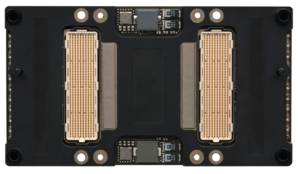
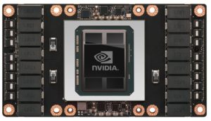
Tesla P100 tackles both memory challenges using stacked memory, a technology which enables multiple layers of DRAM components to be integrated vertically on the package along with the GPU. Tesla P100 is the first GPU accelerator to use High Bandwidth Memory 2 (HBM2). HBM2 memory provides much greater bandwidth, more than twice the capacity, and higher energy efficiency, compared to current off-package GDDR5.
Rather than requiring numerous discrete memory chips surrounding the GPU as in traditional GDDR5 GPU board designs, HBM2 includes one or more vertical stacks of multiple memory dies. The memory dies are linked using tiny wires that are called through-silicon vias and microbumps. One 8 Gb HBM2 die contains over 5,000 through-silicon via holes. A passive silicon interposer is then used to connect the memory stacks and the GPU die. The combination of HBM2 stacks, GPU die, and silicon interposer are packaged in a single 55mm x 55mm BGA package.
Tesla P100 accelerators have four 4-die HBM2 stacks, for a total of 16 GB of memory, and 720 GB/s peak bandwidth, which is 3 times higher than the Tesla M40 memory bandwidth.
ECC Memory
Another HBM2 benefit is native support for error correcting code (ECC) funtionality, which provides higher reliability for technical computing applications that are sensitive to data corruption, such as in large-scale clusters and supercomputers, where GPUs process large datasets with long application run times.
ECC technology detects and corrects single-bit soft errors before they affect the system. In comparison, GDDR5 does not provide internal ECC protection of the contents of memory and is limited to error detection of the GDDR5 bus only: Errors in the memory controller or the DRAM itself are not detected.
GK110 Kepler GPUs offered ECC protection for GDDR5 by allocating some of the available memory for explicit ECC storage. 6.25% of the overall GDDR5 is reserved for ECC bits. In the case of a 12 GB Tesla K40 (for example), 750 MB of its total memory is reserved for ECC operation, resulting in 11.25 GB (out of 12 GB) of available memory with ECC turned on for Tesla K40. Also, accessing ECC bits causes a small decrease in memory bandwidth compared to the non-ECC case. Since HBM2 supports ECC natively, Tesla P100 does not suffer from the capacity overhead, and ECC can be active at all times without a bandwidth penalty. Like the GK110 GPU, the GP100 GPU’s register files, shared memories, L1 cache, L2 cache, and the Tesla P100 accelerator’s HBM2 DRAM are protected by a Single‐Error Correct Double‐Error Detect (SECDED) ECC code.
NVLink High Speed Interconnect
NVLink is NVIDIA’s new high-speed interconnect technology for GPU-accelerated computing. Supported on SXM-2 based Tesla P100 accelerator boards, NVLink significantly increases performance for both GPU-to-GPU communications, and for GPU access to system memory.
Today, multiple GPUs are common in workstations as well as the nodes of HPC computing clusters and deep learning training systems. A powerful interconnect is extremely valuable in multiprocessing systems. Our vision for NVLink was to create an interconnect for GPUs that would offer much higher bandwidth than PCI Express Gen 3 (PCIe), and be compatible with the GPU ISA to support shared memory multiprocessing workloads.
Support for the GPU ISA means that programs running on NVLink-connected GPUs can execute directly on data in the memory of another GPU as well as on local memory. GPUs can also perform atomic memory operations on remote GPU memory addresses, enabling much tighter data sharing and improved application scaling.
NVLink uses NVIDIA’s new High-Speed Signaling interconnect (NVHS). NVHS transmits data over a differential pair running at up to 20 Gb/sec. Eight of these differential connections form a “Sub-Link” that sends data in one direction, and two sub-links—one for each direction—form a “Link” that connects two processors (GPU-to-GPU or GPU-to-CPU). A single Link supports up to 40 GB/sec of bidirectional bandwidth between the endpoints. Multiple Links can be combined to form “Gangs” for even higher-bandwidth connectivity between processors. The NVLink implementation in Tesla P100 supports up to four Links, allowing for a gang with an aggregate maximum theoretical bandwidth of 160 GB/sec bidirectional bandwidth.
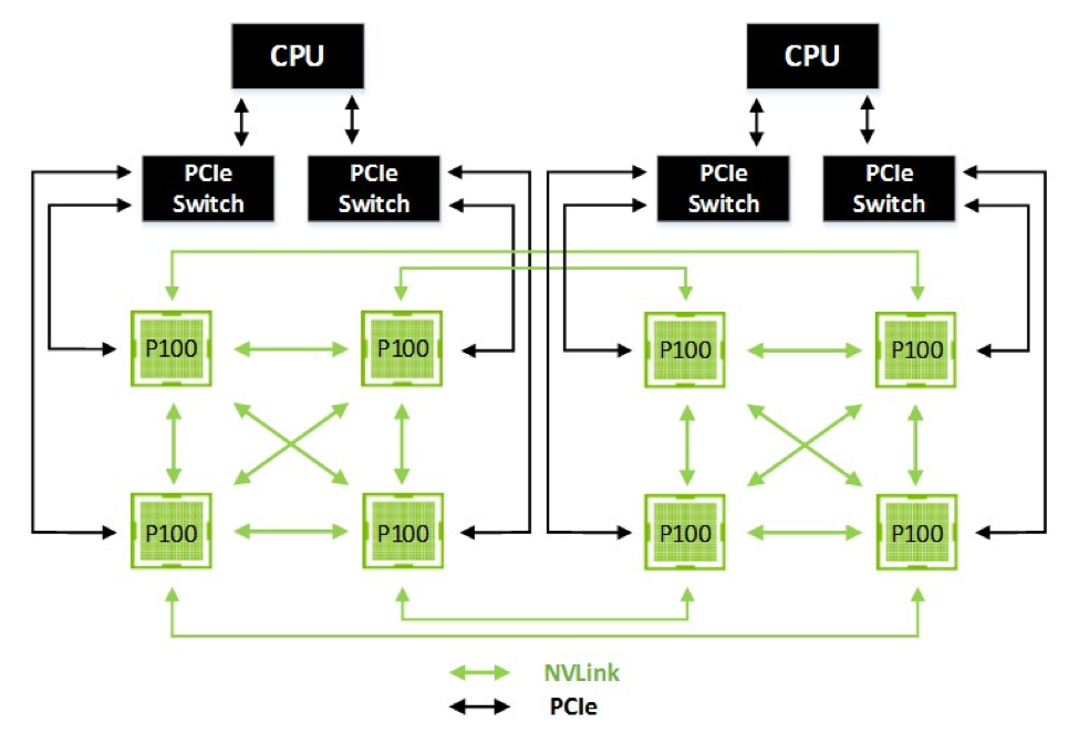
The figure below shows an 8-GPU Hybrid Cube Mesh that includes two fully NVLink-connected quads of GPUs, with NVLink connections between the quads, and GPUs within each quad connected to their respective CPUs directly through PCIe.
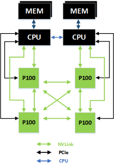
While NVLink primarily focuses on connecting multiple NVIDIA Pascal GP100 GPUs together it can also connect Pascal GP100 GPUs with IBM Power CPUs with NVLink support. The following figure highlights an example of a four-GPU system with dual NVLink-capable CPUs connected with NVLink. In this configuration, each GPU has 120 combined GB/s bidirectional bandwidth to the other 3 GPUs in the system, and 40 GB/s bidirectional bandwidth to a CPU.
Increasing Developer Productivity with Unified Memory
Unified Memory is an important feature of the CUDA programming model that greatly simplifies programming and porting of applications to GPUs by providing a single, unified virtual address space for accessing all CPU and GPU memory in the system. Pascal GP100 features provide a significant advancement for GPU computing by expanding the capabilities and improving the performance of Unified Memory.
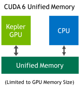
CUDA 6 introduced Unified Memory, which creates a pool of managed memory that is shared between the CPU and GPU, bridging the CPU-GPU divide. Managed memory is accessible to both the CPU and GPU using a single pointer. The CUDA system software automatically migrates data allocated in Unified Memory between GPU and CPU, so that it looks like CPU memory to code running on the CPU, and like GPU memory to code running on the GPU. For more information about how Unified Memory in CUDA 6 and later simplifies porting code to the GPU, see Unified Memory in CUDA 6.
CUDA 6 Unified Memory was limited by the features of the Kepler and Maxwell GPU architectures: all managed memory touched by the CPU had to be synchronized with the GPU before any kernel launch; the CPU and GPU could not simultaneously access a managed memory allocation; and the Unified Memory address space was limited to the size of the GPU physical memory.
Pascal GP100 Unified Memory
Expanding on the benefits of CUDA 6 Unified Memory, Pascal GP100 adds features to further simplify programming and sharing of memory between CPU and GPU, and allowing easier porting of CPU parallel compute applications to use GPUs for tremendous speedups. Two main hardware features enable these improvements: support for large address spaces and page faulting capability.
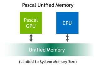
GP100 extends GPU addressing capabilities to enable 49-bit (512 TB) virtual memory addressing (note that GP100 also supports 47-bit (128 TB) physical memory addressing). This is large enough to cover the 48-bit virtual address spaces of modern CPUs, as well as the GPU’s own memory. Therefore, GP100 Unified Memory allows programs to access the full address spaces of all CPUs and GPUs in the system as a single virtual address space, unlimited by the physical memory size of any one processor.
Memory page faulting support in GP100 is a crucial new feature that provides more seamless Unified Memory functionality.
Combined with the system-wide virtual address space, page faulting provides several benefits.
- Page faulting means that the CUDA system software doesn’t need to synchronize all managed memory allocations to the GPU before each kernel launch. If a kernel running on the GPU accesses a page that is not resident in its memory, it faults, allowing the page to be automatically migrated to the GPU memory on-demand.
- The page may be mapped into the GPU address space for access over the PCIe or NVLink interconnects (mapping on access can sometimes be faster than migration).
Unified Memory is system-wide: GPUs (and CPUs) can fault on and migrate memory pages either from CPU memory or from the memory of other GPUs in the system.
With the new page fault mechanism, global data coherency is guaranteed with Unified Memory. This means that with GP100, the CPUs and GPUs can access Unified Memory allocations simultaneously. This was illegal on Kepler and Maxwell GPUs, because coherence could not be guaranteed if the CPU accessed a Unified Memory allocation while a GPU kernel was active. As with any parallel application, you must ensure correct synchronization to avoid data hazards between processors.
Finally, on supporting platforms, memory allocated with the default OS allocator (e.g. malloc or new) can be accessed from both GPU code and CPU code using the same pointer (see the following code example).
On these systems, Unified Memory is the default: there is no need to use a special allocator or for the creation of a special managed memory pool. Moreover, GP100’s large virtual address space and page faulting capability enable applications to access the entire system virtual memory. This means that applications can oversubscribe the memory system. In other words, they can allocate, access, and share arrays larger than the total physical capacity of the system, enabling out-of-core processing of large datasets.
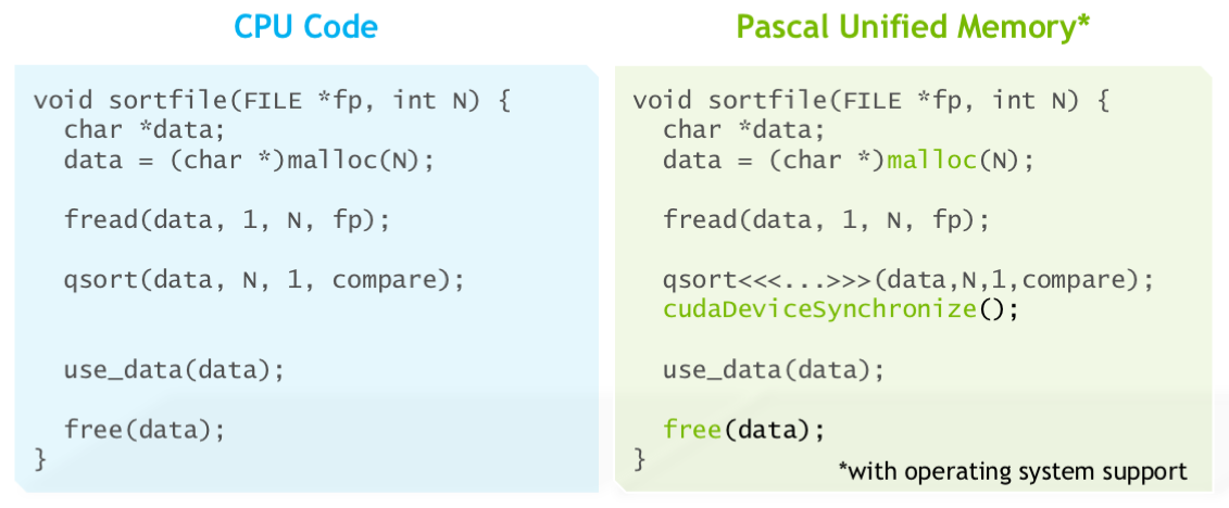
Certain operating system modifications are required to enable Unified Memory with the system allocator. NVIDIA is collaborating with Red Hat and working within the Linux community to enable this powerful functionality.
NVIDIA DGX-1 Deep Learning Supercomputer
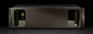
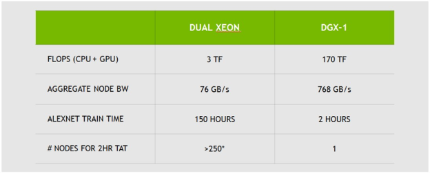
Data scientists and artificial intelligence (AI) researchers require accuracy, simplicity, and speed from their Deep Learning systems. Faster training and iteration ultimately mean faster innovation and faster time to market. The NVIDIA DGX-1 is the world’s first purpose-built server for Deep Learning, with fully integrated hardware and software that can be deployed quickly and easily. Its revolutionary performance of up to 170 FP16 TFLOP/s significantly accelerates training time, making the NVIDIA DGX-1 the first “AI supercomputer in a box”.
The NVIDIA DGX-1 server is the first server using Tesla P100 accelerators interconnected with NVLink. Available in an eight (8) Tesla P100 accelerator configuration, the DGX-1 system is built with high performance/high-reliability components in a 3U rack-mountable chassis for standalone use or cluster integration.
The 8-GPU configuration features two NVLink fully-connected P100 GPU quads that are tied together by four additional NVLinks in a Hybrid Cube Mesh topology (See the 8-GPU NVLink diagram above). Every GPU in a quad is also directly connected via PCIe to a PCIe switch that connects to a CPU. The bottom line is that an NVIDIA DGX-1 server with eight Tesla P100 accelerators can deliver over 12x the Deep Learning performance compared to previous GPU-accelerated solutions.
Combining powerful hardware with software tailored to Deep Learning, the NVIDIA DGX-1 enables developers and researchers with a turnkey solution for high-performance GPU-accelerated Deep Learning application development, testing, and network training.
Tesla P100: Built for HPC and Deep Learning
As you can see, the new NVIDIA Tesla P100 accelerator is a performance powerhouse with revolutionary new features for technical computing and deep learning. Faster in every way than its predecessors, Tesla P100 provides massive leaps in computational throughput, memory bandwidth and capacity, interconnect performance, and programmability.
In this post, I’ve really only scratched the surface—there are many more new features in the Pascal GP100 architecture and in Tesla P100, including new instructions, powerful features such as compute preemption, and more that I couldn’t fit into this post. To learn more, read the Tesla P100 white paper and check out “Inside Pascal” from GTC 2016.
This post was first published April 5, 2016, and updated June 19, 2016 with information on Tesla P100 for PCIe.
